


 Trouble in Your Tank: Implementing Direct Metallization in Advanced Substrate Packaging
 It’s Only Common Sense: Storytelling That Sells—Stop Pitching, Start Painting Pictures
 The Right Approach: Get Ready for ISO 9001 Version 6


Switch Controls Light on a Nanoscale for Faster Information Processing
May 3, 2018 | Purdue UniversityEstimated reading time: 2 minutes
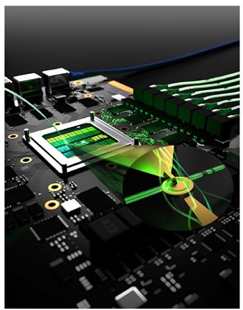
Purdue researchers have helped design a compact switch that enables light to be more reliably confined to small computer chip components for faster information processing.
It’s well known that photons, or units of light, are faster than electrons and could, therefore, process information faster from smaller chip structures. A switch designed in collaboration with researchers from ETH Zürich, the University of Washington and Virginia Commonwealth University bypasses a tendency for the unwanted absorption of light when using so-called surface plasmons, or light coupled to oscillations of free electron clouds, to help confine light to a nanoscale.
“The big idea behind this is going from electronic circuitry to photonic circuitry,” said Vladimir Shalaev, Purdue’s Bob and Anne Burnett Distinguished Professor of Electrical and Computer Engineering. “From electronics to photonics, you need some structures that confine light to be put into very small areas. And plasmonics seems to be the solution.”
Even though plasmonics downsizes light, photons also get lost, or absorbed, rather than transferred to other parts of the computer chip when they interact with plasmons.
In a study publishing April 26 in Nature, researchers addressed this problem through the development of a switch, called a ring modulator, that uses resonance to control whether light couples with plasmons. When on, or out of resonance, light travels through silicon waveguides to other parts of the chip. When off, or in resonance, light couples with plasmons and is absorbed.
“When you have a purely plasmonic device, light can be lossy, but in this case it’s a gain for us because it reduces a signal when necessary,” said Soham Saha, a graduate research assistant in Purdue’s school of electrical and computer engineering. “The idea is to select when you want loss and when you don’t.”
The loss creates a contrast between on and off states, thus better enabling control over the direction of light where appropriate for processing bits of information. A plasmon-assisted ring modulator also results in a smaller “footprint” because plasmons enable confinement of light down to nanoscale chip structures, Shalaev said.
Purdue researchers plan to make this modulator fully compatible with complementary metal-oxide-semiconductor transistors, paving the way to truly hybrid photonic and electronic nanocircuitry for computer chips.
“Supercomputers already contain both electronic and optical components to do massive calculations very fast,” said Alexandra Boltasseva, Purdue professor of electrical and computer engineering, whose lab specializes in plasmonic materials. “What we’re working on would fit very well into this hybrid model, so we don’t have to wait to use it when computer chips go all-optical.”
Development of the plasmon assisted electro-optic modulator required expertise in not only plasmonics, but also integrated circuitry and nanophotonics from the leading group of Juerg Leuthold at ETH Zürich – including Christian Haffner and other group members – and in opto-electronic switching materials from Larry Dalton’s group at the University of Washington. Haffner and Nathaniel Kinsey, former Purdue student and now a professor of electrical and computer engineering at Virginia Commonwealth University, along with Leuthold, Shalaev and Boltasseva, conceived the idea of a low-loss plasmon assisted electro-optic modulator for subwavelength optical devices, including compact on-chip sensing and communications technologies.
Share on:


Testimonial
"In a year when every marketing dollar mattered, I chose to keep I-Connect007 in our 2025 plan. Their commitment to high-quality, insightful content aligns with Koh Young’s values and helps readers navigate a changing industry. "
Brent Fischthal - Koh YoungSuggested Items
ASM Technologies Limited signs MoU with the Guidance, Government of Tamilnadu to Expand Design-Led Manufacturing capabilities for ESDM
09/15/2025 | ASM TechnologiesASM Technologies Limited, a pioneer in Design- Led Manufacturing in the semiconductor and automotive industries, announced signing of Memorandum of Understanding (MoU) with the Guidance, Government of Tamilnadu whereby it will invest Rs. 250 crores in the state to expand its ESDM related Design-Led Manufacturing and precision engineering capacity. ASM Technologies will acquire 5 acres of land from the Government of Tamilnadu to set up a state-of-the-art design facility in Tamil Nadu's growing technology manufacturing ecosystem, providing a strong strategic advantage and long-term benefits for ASM.
Intel Announces Key Leadership Appointments to Accelerate Innovation and Strengthen Execution
09/09/2025 | Intel CorporationIntel Corporation today announced a series of senior leadership appointments that support the company’s strategy to strengthen its core product business, build a trusted foundry, and foster a culture of engineering across the business.
Cadence to Acquire Hexagon’s Design & Engineering Business
09/08/2025 | Cadence Design SystemsCadence announced it has entered into a definitive agreement to acquire the Design & Engineering (D&E) business of Hexagon AB, which includes its MSC Software business—a pioneer in engineering simulation and analysis solutions.
Marcy’s Musings: Continuing to Invent the Future With SEL
08/19/2025 | Marcy LaRont -- Column: Marcy's MusingsTwo years ago, PCB007 Magazine devoted an issue to Schweitzer Engineering Labs (SEL), a new captive greenfield PCB facility in Moscow, Idaho. We highlighted some of the most cutting-edge achievements in facility layout, design, and equipment in the PCB fabrication industry. SEL was a shining example of what was possible, providing insight and inspiration to PCB fabricators looking toward growth and expansion.
Advint and SanRex Expand High-Performance DC Rectifier Access for North American PCB Fabricators
08/12/2025 | Advint IncorporatedAdvint Incorporated has entered a strategic partnership with SanRex Corporation, enhancing access to industrial-grade DC rectifiers for the US printed circuit board industry. With a legacy of power innovation and performance across the globe, SanRex rectifiers are available through Advint’s proficient distribution network.