


 Trouble in Your Tank: Implementing Direct Metallization in Advanced Substrate Packaging
 It’s Only Common Sense: Storytelling That Sells—Stop Pitching, Start Painting Pictures
 The Right Approach: Get Ready for ISO 9001 Version 6


Atomically Thin Magnetic Device Could Lead to New Memory Technologies
May 4, 2018 | University of WashingtonEstimated reading time: 3 minutes
Magnetic materials are the backbone of modern digital information technologies, such as hard-disk storage. A University of Washington-led team has now taken this one step further by encoding information using magnets that are just a few layers of atoms in thickness. This breakthrough may revolutionize both cloud computing technologies and consumer electronics by enabling data storage at a greater density and improved energy efficiency.
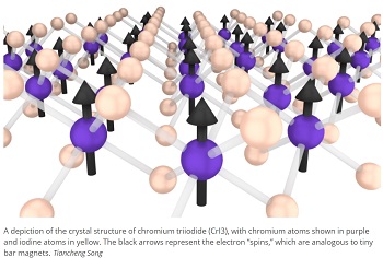
In a study published online May 3 in the journal Science, the researchers report that they used stacks of ultrathin materials to exert unprecedented control over the flow of electrons based on the direction of their spins — where the electron “spins” are analogous to tiny, subatomic magnets. The materials that they used include sheets of chromium tri-iodide (CrI3), a material described in 2017 as the first ever 2-D magnetic insulator. Four sheets — each only atoms thick — created the thinnest system yet that can block electrons based on their spins while exerting more than 10 times stronger control than other methods.
“Our work reveals the possibility to push information storage based on magnetic technologies to the atomically thin limit,” said co-lead author Tiancheng Song, a UW doctoral student in physics.
In related research, published April 23 in Nature Nanotechnology, the team found ways to electrically control the magnetic properties of this atomically thin magnet.
“With the explosive growth of information, the challenge is how to increase the density of data storage while reducing operation energy,” said corresponding author Xiaodong Xu, a UW professor of physics and of materials science and engineering, and faculty researcher at the UW Clean Energy Institute. “The combination of both works points to the possibility of engineering atomically thin magnetic memory devices with energy consumption orders of magnitude smaller than what is currently achievable.”
The new Science paper also looks at how this material could allow for a new type of memory storage that exploits the electron spins in each individual sheet.
The researchers sandwiched two layers of CrI3 between conducting sheets of graphene. They showed that, depending on how the spins are aligned between each of the CrI3 sheets, the electrons can either flow unimpeded between the two graphene sheets or were largely blocked from flowing. These two different configurations could act as the bits — the zeroes and ones of binary code in everyday computing — to encode information.
“The functional units of this type of memory are magnetic tunnel junctions, or MTJ, which are magnetic ‘gates’ that can suppress or let through electrical current depending on how the spins align in the junction,” said co-lead author Xinghan Cai, a UW postdoctoral researcher in physics. “Such a gate is central to realizing this type of small-scale data storage.”
With up to four layers of CrI3, the team discovered the potential for “multi-bit” information storage. In two layers of CrI3, the spins between each layer are either aligned in the same direction or opposite directions, leading to two different rates that the electrons can flow through the magnetic gate. But with three and four layers, there are more combinations for spins between each layer, leading to multiple, distinct rates at which the electrons can flow through the magnetic material from one graphene sheet to the other.
“Instead of your computer having just two choices to store a piece of data in, it can have a choice A, B, C, even D and beyond,” said co-author Bevin Huang, a UW doctoral student in physics. “So not only would storage devices using CrI3 junctions be more efficient, but they would intrinsically store more data.”
The researchers’ materials and approach represent a significant improvement over existing techniques under similar operating conditions using magnesium oxide, which is thicker, less effective at blocking electrons and lacks the option for multi-bit information storage.
“Although our current device requires modest magnetic fields and is only functional at low temperature, infeasible for use in current technologies, the device concept and operational principle are novel and groundbreaking,” said Xu. “We hope that with developed electrical control of magnetism and some ingenuity, these tunnel junctions can operate with reduced or even without the need for a magnetic field at high temperature, which could be a game changer for new memory technology.”
Additional co-authors are Nathan Wilson, Kyle Seyler, Lin Zhu and David Cobden at the UW; co-corresponding author Wang Yao and Matisse Wei-Yuan Tu at the University of Hong Kong; co-corresponding author Di Xiao and Xiao-Ou Zhang at Carnegie Mellon University; Takashi Taniguchi and Kenji Watanabe at the National Institute for Materials Science in Tsukuba, Japan; and Michael McGuire at the Oak Ridge National Laboratory in Tennessee. The major funder of the research were the U.S. Department of Energy. Part of work was performed at the Research Training Testbeds at the Clean Energy Institute.
Share on:


Testimonial
"The I-Connect007 team is outstanding—kind, responsive, and a true marketing partner. Their design team created fresh, eye-catching ads, and their editorial support polished our content to let our brand shine. Thank you all! "
Sweeney Ng - CEE PCBSuggested Items
I-Connect007 Launches Advanced Electronics Packaging Digest
09/15/2025 | I-Connect007I-Connect007 is pleased to announce the launch of Advanced Electronics Packaging Digest (AEPD), a new monthly digital newsletter dedicated to one of the most critical and rapidly evolving areas of electronics manufacturing: advanced packaging at the interconnect level.
Panasonic Industry will Double the Production Capacity of MEGTRON Multi-layer Circuit Board Materials Over the Next Five Years
09/15/2025 | Panasonic Industry Co., Ltd.Panasonic Industry Co., Ltd., a Panasonic Group company, announced plans for a major expansion of its global production capacity for MEGTRON multi-layer circuit board materials today. The company plans to double its production over the next five years to meet growing demand in the AI server and ICT infrastructure markets.
Trouble in Your Tank: Implementing Direct Metallization in Advanced Substrate Packaging
09/15/2025 | Michael Carano -- Column: Trouble in Your TankDirect metallization systems based on conductive graphite are gaining popularity throughout the world. The environmental and productivity gains achievable with this process are outstanding. Direct metallization reduces the costs of compliance, waste treatment, and legal issues related to chemical exposure. A graphite-based direct plate system has been devised to address these needs.
Fresh PCB Concepts: Designing for Success at the Rigid-flex Transition Area
08/28/2025 | Team NCAB -- Column: Fresh PCB ConceptsRigid-flex PCBs come in all shapes and sizes. Manufacturers typically use fire-retardant, grade 4 (FR-4) materials in the rigid section and flexible polyimide materials in the flex region. Because of the small size, some rigid-flex PCBs, like those for hearing aid devices, are among the most challenging to manufacture. However, regardless of its size, we should not neglect the transition area between the rigid and flexible material.
Global Sourcing Spotlight: How to Evaluate Supplier Capabilities Worldwide
08/20/2025 | Bob Duke -- Column: Global Sourcing SpotlightIn global sourcing, the difference between a competitive edge and a catastrophic disruption often comes down to how well you vet your suppliers. Sourcing advanced PCBs, precision components, or materials for complex assemblies demands diligence, skepticism, and more than a little time on airplanes. Here’s how to do your due diligence when evaluating international suppliers and why cutting corners can cost you more than money.