


 Trouble in Your Tank: Implementing Direct Metallization in Advanced Substrate Packaging
 It’s Only Common Sense: Storytelling That Sells—Stop Pitching, Start Painting Pictures
 The Right Approach: Get Ready for ISO 9001 Version 6


A Surprising New Superconductor
May 11, 2018 | CIRESEstimated reading time: 3 minutes
Last September, CIRES chemist and instrument designer Don David and colleagues Dave Pappas and Xian Wu at the National Institute of Standards and Technology discovered a powerful new plated metal combination that superconducts at easily attained temperatures—paving the road for the next critical steps in the development of cutting-edge supercomputers. David and his colleagues just published the new recipe: an ultrathin layer of rhenium sandwiched between layers of gold, each measuring 1/1000th the diameter of a human hair that can superconduct at critical temperature over 6 Kelvin.
“The sheer magnitude of the critical temperature was unexpected,” said Don David, director of the CIRES Integrated Instrument Development Facility and coauthor on a paper published this week in Applied Physics Letters. “We had been thinking for a while about ways to impart superconducting properties to gold and copper films, and we were surprised at how robust and effective the thin layer of electroplated Re was.”
A superconductor is a material with zero electrical resistance when cooled to a critical temperature. This temperature is usually strikingly low and expensive to obtain. The team’s electroplated rhenium meets ideal characteristics desired for use in circuit boards for ultrafast, next-generation computing applications: superconducting at higher, easier-to-achieve critical temperatures, easy to work with mechanically, non-toxic, and melts at high temperatures. The new finding is already drawing attention from international computing giants.
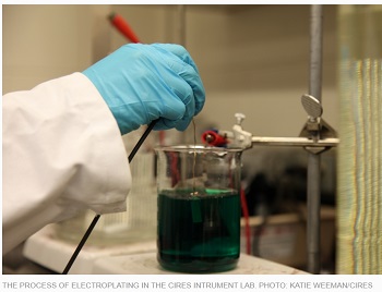
Electroplating, the process passing an electrical current through an aqueous solution of a dissolved metal to create a metal coating on a submerged object, is something David does almost daily. David’s work is in high demand in the research community: He and his team support science by plating instruments like charged-particle optics and components for cryogenics applications, and in this case, circuit boards for a team at NIST. They were looking for a metal plating that might be superconducting for the Pappas’s Quantum Processing Group at NIST. The team had unsuccessfully tried a number combinations, then one day David’s NIST colleague Xian Wu suggested they try rhenium: a hard, trace metal, with a high melting point, often used in the construction of jet engine turbines.
The team tested for electrical resistance, and were happy to see it superconduct up to 6K, well above the boiling temperature of liquid helium (4.2 K). The team is now investigating the role of hydrogen incorporation, interfaces, and strain on the enhanced superconducting temperature. But whatever the reason for the enhancement, being able to electroplate a superconductor is a giant step forward in the creation of tomorrow’s high-performance, superconducting computers.
Inside every computer there is a circuit board: a layered, electronic plank etched with thousands of conductive pathways. Pulses of electrical information called “bits” speed across the board, carrying out the computer’s functions. In regular computers, these electrical pulses are hindered by the material that comprises the board—electrical resistance slows down the electrons scurrying about the circuitry, and the wasted energy becomes heat. But with a superconductor, there is literally zero electrical resistance, so there is no heating. This efficiency will result in exceedingly fast and powerful computer systems.
Superconductors aren’t new, but the new paper presents evidence that electroplated rhenium may be the best material found to date for superconductive computer circuit board construction. Many other superconductive materials, like mercury or lead, are difficult to work with mechanically, have poor soldering properties, or melt at too-low temperatures. Even more impressively, the electroplating process would be easily scaled-up to mass-production, David said.
The team has applied for a provisional patent, and their work has already sparked interest from several technology giants and government sponsors.
Share on:


Testimonial
"We’re proud to call I-Connect007 a trusted partner. Their innovative approach and industry insight made our podcast collaboration a success by connecting us with the right audience and delivering real results."
Julia McCaffrey - NCAB GroupSuggested Items
Trouble in Your Tank: Implementing Direct Metallization in Advanced Substrate Packaging
09/15/2025 | Michael Carano -- Column: Trouble in Your TankDirect metallization systems based on conductive graphite are gaining popularity throughout the world. The environmental and productivity gains achievable with this process are outstanding. Direct metallization reduces the costs of compliance, waste treatment, and legal issues related to chemical exposure. A graphite-based direct plate system has been devised to address these needs.
Closing the Loop on PCB Etching Waste
09/09/2025 | Shawn Stone, IECAs the PCB industry continues its push toward greener, more cost-efficient operations, Sigma Engineering’s Mecer System offers a comprehensive solution to two of the industry’s most persistent pain points: etchant consumption and rinse water waste. Designed as a modular, fully automated platform, the Mecer System regenerates spent copper etchants—both alkaline and acidic—and simultaneously recycles rinse water, transforming a traditionally linear chemical process into a closed-loop system.
Driving Innovation: Depth Routing Processes—Achieving Unparalleled Precision in Complex PCBs
09/08/2025 | Kurt Palmer -- Column: Driving InnovationIn PCB manufacturing, the demand for increasingly complex and miniaturized designs continually pushes the boundaries of traditional fabrication methods, including depth routing. Success in these applications demands not only on robust machinery but also sophisticated control functions. PCB manufacturers rely on advanced machine features and process methodologies to meet their precise depth routing goals. Here, I’ll explore some crucial functions that empower manufacturers to master complex depth routing challenges.
Trouble in Your Tank: Minimizing Small-via Defects for High-reliability PCBs
08/27/2025 | Michael Carano -- Column: Trouble in Your TankTo quote the comedian Stephen Wright, “If at first you don’t succeed, then skydiving is not for you.” That can be the battle cry when you find that only small-diameter vias are exhibiting voids. Why are small holes more prone to voids than larger vias when processed through electroless copper? There are several reasons.
The Government Circuit: Navigating New Trade Headwinds and New Partnerships
08/25/2025 | Chris Mitchell -- Column: The Government CircuitAs global trade winds continue to howl, the electronics manufacturing industry finds itself at a critical juncture. After months of warnings, the U.S. Government has implemented a broad array of tariff increases, with fresh duties hitting copper-based products, semiconductors, and imports from many nations. On the positive side, tentative trade agreements with Europe, China, Japan, and other nations are providing at least some clarity and counterbalance.