


 Trouble in Your Tank: Implementing Direct Metallization in Advanced Substrate Packaging
 It’s Only Common Sense: Storytelling That Sells—Stop Pitching, Start Painting Pictures
 The Right Approach: Get Ready for ISO 9001 Version 6


Chemists Create Faster and More Efficient Way to Process Information
May 11, 2018 | University of WaterlooEstimated reading time: 1 minute
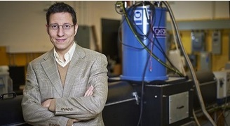
University of Waterloo chemists have found a much faster and more efficient way to store and process information by expanding the limitations of how the flow of electricity can be used and managed.
In a recently released study, the chemists discovered that light can induce magnetization in certain semiconductors - the standard class of materials at the heart of all computing devices today.
"These results could allow for a fundamentally new way to process, transfer, and store information by electronic devices, that is much faster and more efficient than conventional electronics."
For decades, computer chips have been shrinking thanks to a steady stream of technological improvements in processing density. Experts have, however, been warning that we'll soon reach the end of the trend known as Moore's Law, in which the number of transistors per square inch on integrated circuits double every year.
"Simply put, there's a physical limit to the performance of conventional semiconductors as well as how dense you can build a chip," said Pavle Radovanovic, a professor of chemistry and a member of the Waterloo Institute for Nanotechnology. "In order to continue improving chip performance, you would either need to change the material transistors are made of - from silicon, say to carbon nanotubes or graphene - or change how our current materials store and process information."
Radovanovic's finding is made possible by magnetism and a field called spintronics, which proposes to store binary information within an electron's spin direction, in addition to its charge and plasmonics, which studies collective oscillations of elements in a material.
"We've basically magnetized individual semiconducting nanocrystals (tiny particles nearly 10,000 times smaller than the width of a human hair) with light at room temperature," said Radovanovic. "It's the first time someone's been able to use collective motion of electrons, known as plasmon, to induce a stable magnetization within such a non-magnetic semiconductor material."
In manipulating plasmon in doped indium oxide nanocrystals Radovanovic's findings proves that the magnetic and semiconducting properties can indeed be coupled, all without needing ultra-low temperatures (cryogens) to operate a device.
He anticipates the findings could initially lead to highly sensitive magneto-optical sensors for thermal imaging and chemical sensing. In the future, he hopes to extend this approach to quantum sensing, data storage, and quantum information processing.
Share on:


Testimonial
"Advertising in PCB007 Magazine has been a great way to showcase our bare board testers to the right audience. The I-Connect007 team makes the process smooth and professional. We’re proud to be featured in such a trusted publication."
Klaus Koziol - atgSuggested Items
Sustainability and Selective Soldering
09/15/2025 | Dr. Samuel J. McMaster, Pillarhouse InternationalSustainability is more than just a buzzword for the electronics industry; it’s a key goal for all manufacturing processes. This is more than a box-ticking exercise or simply doing a small part for environmentally friendly processes. Moving toward sustainable solutions drives innovation and operational efficiency.
Trouble in Your Tank: Implementing Direct Metallization in Advanced Substrate Packaging
09/15/2025 | Michael Carano -- Column: Trouble in Your TankDirect metallization systems based on conductive graphite are gaining popularity throughout the world. The environmental and productivity gains achievable with this process are outstanding. Direct metallization reduces the costs of compliance, waste treatment, and legal issues related to chemical exposure. A graphite-based direct plate system has been devised to address these needs.
EV Group Achieves Breakthrough in Hybrid Bonding Overlay Control for Chiplet Integration
09/12/2025 | EV GroupEV Group (EVG), a leading provider of innovative process solutions and expertise serving leading-edge and future semiconductor designs and chip integration schemes, today unveiled the EVG®40 D2W—the first dedicated die-to-wafer overlay metrology platform to deliver 100 percent die overlay measurement on 300-mm wafers at high precision and speeds needed for production environments. With up to 15X higher throughput than EVG’s industry benchmark EVG®40 NT2 system designed for hybrid wafer bonding metrology, the new EVG40 D2W enables chipmakers to verify die placement accuracy and take rapid corrective action, improving process control and yield in high-volume manufacturing (HVM).
Integrating Uniplate PLBCu6 With the Digital Factory Suite
09/12/2025 | Giovanni Obino and Andreas Schatz, MKS' AtotechPrinted circuit board manufacturing is rapidly changing, driven by miniaturization, stringent reliability requirements, and growing pressure for sustainable production. Meeting these challenges requires more than incremental improvements; it demands a combination of precise equipment and real-time process intelligence. The pairing of Uniplate® PLBCu6 with the Digital Factory Suite (DFS) demonstrates how hardware and software can work together to create more responsive, resource-efficient manufacturing.
Closing the Loop on PCB Etching Waste
09/09/2025 | Shawn Stone, IECAs the PCB industry continues its push toward greener, more cost-efficient operations, Sigma Engineering’s Mecer System offers a comprehensive solution to two of the industry’s most persistent pain points: etchant consumption and rinse water waste. Designed as a modular, fully automated platform, the Mecer System regenerates spent copper etchants—both alkaline and acidic—and simultaneously recycles rinse water, transforming a traditionally linear chemical process into a closed-loop system.