


 Trouble in Your Tank: Implementing Direct Metallization in Advanced Substrate Packaging
 It’s Only Common Sense: Storytelling That Sells—Stop Pitching, Start Painting Pictures
 The Right Approach: Get Ready for ISO 9001 Version 6


Engineers on a Roll Toward Smaller, More Efficient Radio Frequency Transformers
May 15, 2018 | University of Illinois at Urbana-ChampaignEstimated reading time: 2 minutes
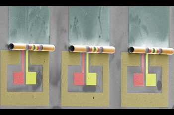
The future of electronic devices lies partly within the "internet of things" - the network of devices, vehicles and appliances embedded within electronics to enable connectivity and data exchange. University of Illinois engineers are helping realize this future by minimizing the size of one notoriously large element of integrated circuits used for wireless communication - the transformer.
Three-dimensional rolled-up radio frequency transformers take 10 to 100 times less space, perform better when the power transfer ratio increases and have a simpler fabrication process than their 2-D progenitors, according to a paper detailing their design and performance in the journal Nature Electronics.
"Transformers are one of the largest and heaviest elements on any circuit board," said principal investigator Xiuling Li, a professor of electrical and computer engineering. "When you pick up an LED light bulb, it feels heavy for its size and that is in part because of the bulky transformer inside. The size of these transformers may become a key obstacle to overcome in the future for wireless communication and IoT."
Transformers use coiled wires to convert input signals to specific output signals for use in devices like microchips. Previous researchers have developed some radio frequency transformers using a stacked conducting material to solve the space problem, but these have limited performance potential. This limited performance is due to inefficient magnetic coupling between coils when they have a high turns ratio, meaning that the primary coil is much longer than the secondary coil, or vice versa, Li said. These stacked transformers need to be made using special materials and are difficult to fabricate, bulky and unbendable - things that are far from ideal for internet of things devices.
The new transformer design uses techniques Li's group previously developed for making rolled inductors. "We are making 3-D structures using 2-D processing," Li said. The team deposits carefully patterned metal wires onto stretched 2-D thin films. Once they release the tension, the 2-D films self-roll into tiny tubes, allowing the primary and secondary wires to coil and nest perfectly inside each other into a much smaller area for optimum magnetic induction and coupling.
The nested 3-D architecture leads to high turns ratio coils, Li said. "A high turns ratio transformer can be used as an impedance transformer to improve the sensitivity of extremely low power receivers, which are expected to be a key enabler for IoT wireless front ends," said electrical and computer engineering professor and co-author Songbin Gong.
Rolled transformers can also receive and process higher frequency signals than the larger devices.
"Wireless communication will be faster and use higher-frequency signals in the future. The current generation of radio frequency transformers simply cannot keep up with the miniaturization requirements and high-frequency operation of the future," said lead author and postdoctoral researcher Wen Huang. "Smaller transformers with more turns allow for better reception of faster, high-frequency wireless signals, as well as high-level integration in IoT applications."
The new transformers have a robust fabrication process - stable beyond standard foundry temperatures and compatible with industry-standard materials. This study used gold wire, but the team has successfully demonstrated the fabrication of their rolled devices using industry-standard copper.
"The next step will be to use thinner and more-conductive metal such as graphene, allowing these devices to be made even smaller and more flexible. This advancement may make it possible for the devices to be woven into the fabrics of high-tech wearables," Li said.
Share on:


Testimonial
"Advertising in PCB007 Magazine has been a great way to showcase our bare board testers to the right audience. The I-Connect007 team makes the process smooth and professional. We’re proud to be featured in such a trusted publication."
Klaus Koziol - atgSuggested Items
Trouble in Your Tank: Implementing Direct Metallization in Advanced Substrate Packaging
09/15/2025 | Michael Carano -- Column: Trouble in Your TankDirect metallization systems based on conductive graphite are gaining popularity throughout the world. The environmental and productivity gains achievable with this process are outstanding. Direct metallization reduces the costs of compliance, waste treatment, and legal issues related to chemical exposure. A graphite-based direct plate system has been devised to address these needs.
Closing the Loop on PCB Etching Waste
09/09/2025 | Shawn Stone, IECAs the PCB industry continues its push toward greener, more cost-efficient operations, Sigma Engineering’s Mecer System offers a comprehensive solution to two of the industry’s most persistent pain points: etchant consumption and rinse water waste. Designed as a modular, fully automated platform, the Mecer System regenerates spent copper etchants—both alkaline and acidic—and simultaneously recycles rinse water, transforming a traditionally linear chemical process into a closed-loop system.
Driving Innovation: Depth Routing Processes—Achieving Unparalleled Precision in Complex PCBs
09/08/2025 | Kurt Palmer -- Column: Driving InnovationIn PCB manufacturing, the demand for increasingly complex and miniaturized designs continually pushes the boundaries of traditional fabrication methods, including depth routing. Success in these applications demands not only on robust machinery but also sophisticated control functions. PCB manufacturers rely on advanced machine features and process methodologies to meet their precise depth routing goals. Here, I’ll explore some crucial functions that empower manufacturers to master complex depth routing challenges.
Trouble in Your Tank: Minimizing Small-via Defects for High-reliability PCBs
08/27/2025 | Michael Carano -- Column: Trouble in Your TankTo quote the comedian Stephen Wright, “If at first you don’t succeed, then skydiving is not for you.” That can be the battle cry when you find that only small-diameter vias are exhibiting voids. Why are small holes more prone to voids than larger vias when processed through electroless copper? There are several reasons.
The Government Circuit: Navigating New Trade Headwinds and New Partnerships
08/25/2025 | Chris Mitchell -- Column: The Government CircuitAs global trade winds continue to howl, the electronics manufacturing industry finds itself at a critical juncture. After months of warnings, the U.S. Government has implemented a broad array of tariff increases, with fresh duties hitting copper-based products, semiconductors, and imports from many nations. On the positive side, tentative trade agreements with Europe, China, Japan, and other nations are providing at least some clarity and counterbalance.