


 Global PCB Connections: Rigid-flex and Flexible PCBs—The Backbone of Modern Electronics
 Flexible Thinking: The Key to a Successful Flex Circuit Design Transfer
 Happy’s Tech Talk #29: Bend-to-Install Semi-flex FR-4


Atotech to Present New Flex, Flex-Rigid Products at C’Tex 2018
May 15, 2018 | AtotechEstimated reading time: 2 minutes
Atotech will showcase its latest production solutions for advanced HDI, flex, and flex-rigid PCBs in hall C1, booth AN6 at the C’Tex 2018 show. The trade show will be held in the Suzhou International Expo Center from May 16-18. Next to its product promotion at its trade show booth, the company takes part in the New Product Introduction sessions with the introduction of its new InPro THF chemistry.
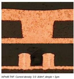
On Thursday, May 17, from 2:00 to 2:40 pm, Mustafa Oezkoek, Global Product Manager for Panel and Pattern Plating at Atotech Deutschland GmbH, will present InPro THF for advanced HDI (mSAP). InPro THF provides reliable BMV filling performance at high current densities up to 3 A/dm² especially for mSAP applications in mass production. The process meets the technological and yield requirements for next generation HDI and packaging and provides pattern plating with excellent pattern distribution. It may also be used for TH filling and reduces the number of processing steps needed, thereby leading to improved reliability, productivity, and reduced costs. The three additive component system further provides excellent stability without the formation of harmful breakdown products.
InPro THF: Current density: 3.0 A/dm², dimple < 3μm
Additional product highlights at Atotech’s booth will be Cupracid Flex / InPro Flex, an economic conformal plating solution for standard flex and rigid-flex applications, and Stanna-COF, an immersion tin for chip on film technology.
Cupracid Flex / InPro Flex
Cupracid Flex and InPro Flex are specifically designed for standard conformal flex applications. The Cupracid Flex process is for use in vertical systems with soluble anodes whereas InPro Flex can be used in systems with insoluble anodes. Even at higher current density, pattern uniformity and line shape are very good. Both processes consist of a simple two additive system and provide excellent throwing power at high current densities without any corner flattening.
Stanna-COF
Stanna-COF is the latest extension to Atotech’s already well versed immersion tin family. The application enables Chip On Film (COF) technology. With Stanna-COF, the chips are bonded straight onto the tracks necessitating a smooth and even finish. The process assures improved yields and functionality and allows for high volume reel to reel production. Stanna-COF has the potential to enhance fine line capability and provides a protective and functional final finish as demanded by this technology.
For further information on these new products, visitors to the show are invited to join Atotech’s New Product Introduction presentation or pass by the Atotech booth in hall C1 number AN6 during the C’Tex show from May 16 to 18. Local and international product specialists will be on site to discuss any question or inquiry.
About Atotech
Atotech is one of the world’s leading manufacturers of specialty chemicals and equipment for the printed circuit board, IC substrate and semiconductor industries, as well as for the decorative and functional surface finishing industries. Atotech has annual sales of USD1.2 billion (2017). The company is fully committed to sustainability – we develop technologies to minimize waste and to reduce environmental impact. Atotech has its headquarters in Berlin, Germany, and employs about 4,000 people in over 40 countries. About a quarter of all staff works in one of the four locations in Germany: Berlin, Feucht, Neuruppin, and Trebur. For more information, click here.
Share on:


Testimonial
"The I-Connect007 team is outstanding—kind, responsive, and a true marketing partner. Their design team created fresh, eye-catching ads, and their editorial support polished our content to let our brand shine. Thank you all! "
Sweeney Ng - CEE PCBSuggested Items
Closing the Loop on PCB Etching Waste
09/09/2025 | Shawn Stone, IECAs the PCB industry continues its push toward greener, more cost-efficient operations, Sigma Engineering’s Mecer System offers a comprehensive solution to two of the industry’s most persistent pain points: etchant consumption and rinse water waste. Designed as a modular, fully automated platform, the Mecer System regenerates spent copper etchants—both alkaline and acidic—and simultaneously recycles rinse water, transforming a traditionally linear chemical process into a closed-loop system.
The Chemical Connection: Experience and Wisdom Gained by Doing Business
09/03/2025 | Don Ball -- Column: The Chemical ConnectionA well-managed company learns to adjust its strategies and processes based on what it learns during challenging times. The experience gained from making (or losing) a difficult sale is invaluable in adapting new sales and manufacturing processes necessary to make that sale the next time, no matter how painful those new processes might be.
MacDermid Alpha Awarded for Innovation: Driving Process Optimization and Efficiency with Major Indian EMS Provider
08/28/2025 | MacDermid Alpha Electronics SolutionsMacDermid Alpha Electronics Solutions, a leading global supplier of integrated materials for the electronics industry, is recognized by one of India’s top EMS providers, Syrma SGS, with an award for innovation that advanced process optimization, enhanced operational efficiency, and yield gains.
Partnerships Drive Innovation for a Brighter Manufacturing Future
08/26/2025 | Barry Matties, I-Connect007When Schweitzer Engineering Laboratories (SEL) opened its greenfield facility in 2023, it did so with careful attention to choosing its suppliers. In this discussion, Collin Peters, electronics business director for North America at MKS’ Atotech, and Justin Kennedy, manager of engineering at SEL, explore their unique partnership that includes collaborative efforts to develop innovative solutions like the Uniplate® PLBCu6 line.
The Art and Science of PCB Floor Planning: A Comprehensive Guide
08/14/2025 | Cory Grunwald and Jeff Reinhold, Monsoon SolutionsPCB design is an intricate and crucial part of developing electronic products. One of the foundational stages of PCB design is floor planning, a phase where the placement of components and the flow of signals are meticulously mapped out. A good floor plan ensures that the PCB performs well, is easy to manufacture, and meets all mechanical and electrical requirements. We’ll explore the essential aspects of floor planning, from its objectives and process to the challenges that designers face.