


 Trouble in Your Tank: Implementing Direct Metallization in Advanced Substrate Packaging
 It’s Only Common Sense: Storytelling That Sells—Stop Pitching, Start Painting Pictures
 The Right Approach: Get Ready for ISO 9001 Version 6


Porous Materials Make it Possible to Have Nanotechnology Under Control
May 17, 2018 | University of CórdobaEstimated reading time: 1 minute
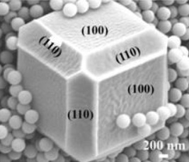
Half metal, half organic structure, like Robocop himself, is the material known as MOF, short for Metal Organic Framework. MOF has been developed by scientists and applied to a myriad of products from sorbents to batteries for electronic devices. This material emerged from the nanotechnology revolution that turned material design upside down and facilitated the improvement of chemical processes. MOFs are a new organic and inorganic hybrid material made up of metallic nodes and organic links characterized by their porosity, that is to say, by the intermolecular spaces that it is comprised of.
The study and understanding of its properties and applicability have centered on recent work by Professor Rafael Luque, of the University of Cordoba Organic Chemistry Department research group FQM-383, and a Southern China Technology University research group, published in Dalton Transactions. The research has proven that in addition to the ability to be used in catalysis processes - by means of which the speed of a chemical reaction is increased - these materials are built as stabilizers of metallic nanostructures. So, it paves the way for working with these kinds of nanoentities, thanks to the control over their stability.
The range of possibilities detailed in Luque's work depend on the encapsulated metal/metallic structure, which could be used for CO2 absorption or steam absorption when working with fuel cells and other kinds of batteries.
The methodology designed by Rafael Luque and his team is considered innovative because it enables control over material design to degrees that were unthinkable before. Previously, these porous materials that can accommodate nanoparticles have been studied, but never before has anyone specified the exact way to thoroughly control all the parameters and make them so pliable.
Diversifying the use of these metal-organic materials as much as possible to take advantage of the stability and pliability that they give to nanostructures will be the main focus for this research group henceforth. This line of research will be described in developing studies that are currently being performed by University of Cordoba research group FQM-383.
Share on:


Testimonial
"Our marketing partnership with I-Connect007 is already delivering. Just a day after our press release went live, we received a direct inquiry about our updated products!"
Rachael Temple - AlltematedSuggested Items
I-Connect007 Launches Advanced Electronics Packaging Digest
09/15/2025 | I-Connect007I-Connect007 is pleased to announce the launch of Advanced Electronics Packaging Digest (AEPD), a new monthly digital newsletter dedicated to one of the most critical and rapidly evolving areas of electronics manufacturing: advanced packaging at the interconnect level.
Panasonic Industry will Double the Production Capacity of MEGTRON Multi-layer Circuit Board Materials Over the Next Five Years
09/15/2025 | Panasonic Industry Co., Ltd.Panasonic Industry Co., Ltd., a Panasonic Group company, announced plans for a major expansion of its global production capacity for MEGTRON multi-layer circuit board materials today. The company plans to double its production over the next five years to meet growing demand in the AI server and ICT infrastructure markets.
Trouble in Your Tank: Implementing Direct Metallization in Advanced Substrate Packaging
09/15/2025 | Michael Carano -- Column: Trouble in Your TankDirect metallization systems based on conductive graphite are gaining popularity throughout the world. The environmental and productivity gains achievable with this process are outstanding. Direct metallization reduces the costs of compliance, waste treatment, and legal issues related to chemical exposure. A graphite-based direct plate system has been devised to address these needs.
Fresh PCB Concepts: Designing for Success at the Rigid-flex Transition Area
08/28/2025 | Team NCAB -- Column: Fresh PCB ConceptsRigid-flex PCBs come in all shapes and sizes. Manufacturers typically use fire-retardant, grade 4 (FR-4) materials in the rigid section and flexible polyimide materials in the flex region. Because of the small size, some rigid-flex PCBs, like those for hearing aid devices, are among the most challenging to manufacture. However, regardless of its size, we should not neglect the transition area between the rigid and flexible material.
Global Sourcing Spotlight: How to Evaluate Supplier Capabilities Worldwide
08/20/2025 | Bob Duke -- Column: Global Sourcing SpotlightIn global sourcing, the difference between a competitive edge and a catastrophic disruption often comes down to how well you vet your suppliers. Sourcing advanced PCBs, precision components, or materials for complex assemblies demands diligence, skepticism, and more than a little time on airplanes. Here’s how to do your due diligence when evaluating international suppliers and why cutting corners can cost you more than money.