


 Driving Innovation: Direct Imaging vs. Conventional Exposure
 It’s Only Common Sense: Selling to Today's Generation of Buyers
 Dan’s Biz Bookshelf: ‘Believe in Better'


Flexible Fingerprint Sensors Promise Embedded Secure Access
May 18, 2018 | Holst CentreEstimated reading time: 2 minutes
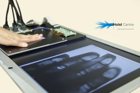
Researchers from Holst Centre have demonstrated a new class of flexible, large-area sensor technology for detecting finger- and palmprints. At less than 0.2 mm thick and with no bulky prisms or moving parts, the new sensors can be embedded into objects such as mobile phones and door handles to create "invisible" yet secure access control systems that can tell if the print is from a living person rather than a phantom or counterfeit.
The technology, which paves the way to low-cost sensors for large-area finger- and palmprint scanners, will be on show at the Innovation Zone at the Society for Information Display (SID) Display Week 2018 in Los Angeles, USA from 22 to 24 May, and the Imec Technology Forum (ITF) in Antwerp, Belgium from 23 to 24 May. Two demonstrators will showcase the technologies potential for high resolution and large active areas.
Measuring 6 x 8 cm, a 200-ppi demonstrator is large enough for 4-finger scanners that are currently used by border control authorities and delivers sufficient image quality for basic identification applications. Meanwhile, a slightly smaller 500-ppi demonstrator offer even higher image quality, compatible with FBI standards and enough for law enforcement agencies to visualize minutia and pores for more robust identification.
As with Holst Centre's earlier flexible X-ray detectors, the fingerprint sensors combine an organic photodiode frontplane, an oxide thin-film transistor (TFT) backplane (originally developed for flexible displays), and a thin-film barrier for protection against the environment. All three technological elements have been or are being transferred to industry for scale-up and commercialization.
The sensors read the finger- or palm print by detecting visible light (400 to 700 nm) reflected from the surface of the skin. However, they can also detect light that penetrates someway into the skin before being reflected. This allows them to sense a heartbeat from changes in the capillaries within the hand, and thus verify that the print comes from a live person.
Moreover, by using different photodiode materials, the sensors' capabilities can be extended to other wavelengths such as near infrared (NIR). This could enable new identification verification modes based on for example the pattern of veins in a hand, which is believed to be even more specific to an individual than a fingerprint. NIR sensors could also be used in other applications, such as blood oxygenation monitoring, or for night vision and 3D facial recognition.
"The flexible fingerprint sensor demonstrator shows the versatility and maturity of the flexible electronics technologies that Holst Centre is developing. With the underlying technology already in use in the flat-panel industry, there is a fast route to manufacturing and we are looking for industrial partners to take that step," says Hylke Akkerman, Program Manager at Holst Centre.
Share on:


Suggested Items
2025 ASEAN IT Spending Growth Slows to 5.9% as AI-Powered IT Expansion Encounters Post-Boom Normalization
06/26/2025 | IDCAccording to the IDC Worldwide Black Book: Live Edition, IT spending across ASEAN is projected to grow by 5.9% in 2025 — down from a robust 15.0% in 2024.
DownStream Acquisition Fits Siemens’ ‘Left-Shift’ Model
06/26/2025 | Andy Shaughnessy, I-Connect007I recently spoke to DownStream Technologies founder Joe Clark about the company’s acquisition by Siemens. We were later joined by A.J. Incorvaia, Siemens’ senior VP of electronic board systems. Joe discussed how he, Rick Almeida, and Ken Tepper launched the company in the months after 9/11 and how the acquisition came about. A.J. provides some background on the acquisition and explains why the companies’ tools are complementary.
United Electronics Corporation Advances Manufacturing Capabilities with Schmoll MDI-ST Imaging Equipment
06/24/2025 | United Electronics CorporationUnited Electronics Corporation has successfully installed the advanced Schmoll MDI-ST (XL) imaging equipment at their advanced printed circuit board facility. This significant technology investment represents a continued commitment to delivering superior products and maintaining their position as an industry leader in precision PCB manufacturing.
Insulectro & Dupont Host Technology Symposium at Silicon Valley Technology Center June 25
06/22/2025 | InsulectroInsulectro, the largest distributor of materials for use in the manufacture of PCBs and printed electronics, and DuPont, a major manufacturer of flex laminates and chemistry, invite fabricators, OEMS, designers, and engineers to attend an Innovation Symposium – Unlock the Power - this Wednesday, June 25, at DuPont’s Silicon Valley Technology Center in Sunnyvale, CA.
OKI, NTT Innovative Devices Establish Mass Production Technology for High-Power Terahertz Devices by Heterogeneous Material Bonding
06/21/2025 | BUSINESS WIREOKI, in collaboration with NTT Innovative Devices Corporation, has established mass production technology for high-power terahertz devices using crystal film bonding (CFB) technology for heterogeneous material bonding to bond indium phosphide (InP)-based uni-traveling carrier photodiodes (UTC-PD) onto silicon carbide (SiC) with excellent heat dissipation characteristics for improved bonding yields.