


 Global PCB Connections: Rigid-flex and Flexible PCBs—The Backbone of Modern Electronics
 Flexible Thinking: The Key to a Successful Flex Circuit Design Transfer
 Happy’s Tech Talk #29: Bend-to-Install Semi-flex FR-4


Flexible Fingerprint Sensors Promise Embedded Secure Access
May 18, 2018 | Holst CentreEstimated reading time: 2 minutes
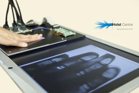
Researchers from Holst Centre have demonstrated a new class of flexible, large-area sensor technology for detecting finger- and palmprints. At less than 0.2 mm thick and with no bulky prisms or moving parts, the new sensors can be embedded into objects such as mobile phones and door handles to create "invisible" yet secure access control systems that can tell if the print is from a living person rather than a phantom or counterfeit.
The technology, which paves the way to low-cost sensors for large-area finger- and palmprint scanners, will be on show at the Innovation Zone at the Society for Information Display (SID) Display Week 2018 in Los Angeles, USA from 22 to 24 May, and the Imec Technology Forum (ITF) in Antwerp, Belgium from 23 to 24 May. Two demonstrators will showcase the technologies potential for high resolution and large active areas.
Measuring 6 x 8 cm, a 200-ppi demonstrator is large enough for 4-finger scanners that are currently used by border control authorities and delivers sufficient image quality for basic identification applications. Meanwhile, a slightly smaller 500-ppi demonstrator offer even higher image quality, compatible with FBI standards and enough for law enforcement agencies to visualize minutia and pores for more robust identification.
As with Holst Centre's earlier flexible X-ray detectors, the fingerprint sensors combine an organic photodiode frontplane, an oxide thin-film transistor (TFT) backplane (originally developed for flexible displays), and a thin-film barrier for protection against the environment. All three technological elements have been or are being transferred to industry for scale-up and commercialization.
The sensors read the finger- or palm print by detecting visible light (400 to 700 nm) reflected from the surface of the skin. However, they can also detect light that penetrates someway into the skin before being reflected. This allows them to sense a heartbeat from changes in the capillaries within the hand, and thus verify that the print comes from a live person.
Moreover, by using different photodiode materials, the sensors' capabilities can be extended to other wavelengths such as near infrared (NIR). This could enable new identification verification modes based on for example the pattern of veins in a hand, which is believed to be even more specific to an individual than a fingerprint. NIR sensors could also be used in other applications, such as blood oxygenation monitoring, or for night vision and 3D facial recognition.
"The flexible fingerprint sensor demonstrator shows the versatility and maturity of the flexible electronics technologies that Holst Centre is developing. With the underlying technology already in use in the flat-panel industry, there is a fast route to manufacturing and we are looking for industrial partners to take that step," says Hylke Akkerman, Program Manager at Holst Centre.
Share on:


Testimonial
"Our marketing partnership with I-Connect007 is already delivering. Just a day after our press release went live, we received a direct inquiry about our updated products!"
Rachael Temple - AlltematedSuggested Items
United Electronics Corporation Unveils Revolutionary CIMS Galaxy 30 Automated Optical Inspection System
09/11/2025 | United Electronics CorporationUnited Electronics Corporation (UEC) today announced the launch of its new groundbreaking CIMS Galaxy 30 Automated Optical Inspection (AOI) machine, setting a new industry standard for precision electronics manufacturing quality control. The Galaxy 30, developed and manufactured by CIMS, represents a significant leap forward in inspection technology, delivering exceptional speed improvements and introducing cutting-edge artificial intelligence capabilities.
Intel Announces Key Leadership Appointments to Accelerate Innovation and Strengthen Execution
09/09/2025 | Intel CorporationIntel Corporation today announced a series of senior leadership appointments that support the company’s strategy to strengthen its core product business, build a trusted foundry, and foster a culture of engineering across the business.
DARPA, State of New Mexico Establish Framework to Advance Quantum Computing
09/08/2025 | DARPAAs part of the Quantum Benchmarking Initiative (QBI), DARPA signed an agreement with the State of New Mexico’s Economic Development Department to create the Quantum Frontier Project.
LPKF Strengthens LIDE Technology Leadership with New Patent Protection in Korea
09/04/2025 | LPKFLPKF Laser & Electronics SE today announced that its groundbreaking LIDE (Laser Induced Deep Etching) technology has received additional patent protection in Korea through the Korean Patent Office (KPCA), effective September 1, 2025.
UHDI Fundamentals: UHDI Technology and Industry 4.0
09/03/2025 | Anaya Vardya, American Standard CircuitsUltra high density interconnect (UHDI) technology is rapidly transforming how smart systems are designed and deployed in the context of Industry 4.0. With its capacity to support highly miniaturized, high-performance, and densely packed electronics, UHDI is a critical enabler of the smart, connected, and automated industrial future. Here, I’ll explore the synergy between UHDI and Industry 4.0 technologies, highlighting applications, benefits, and future directions.