


 Trouble in Your Tank: Implementing Direct Metallization in Advanced Substrate Packaging
 It’s Only Common Sense: Storytelling That Sells—Stop Pitching, Start Painting Pictures
 The Right Approach: Get Ready for ISO 9001 Version 6


Robotic Assembly of the World’s Smallest House
May 21, 2018 | AIP.orgEstimated reading time: 2 minutes
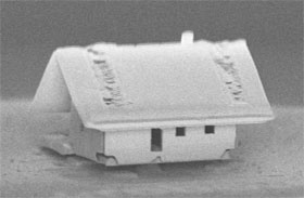
A French nanorobotics team from the Femto-ST Institute in Besançon, France, assembled a new microrobotics system that pushes forward the frontiers of optical nanotechnologies. Combining several existing technologies, the µRobotex nanofactory builds microstructures in a large vacuum chamber and fixes components onto optical fiber tips with nanometer accuracy. The microhouse construction, reported in the Journal of Vacuum Science and Technology A, from AIP Publishing, demonstrates how researchers can advance optical sensing technologies when they manipulate ion guns, electron beams and finely controlled robotic piloting.
Until now, lab-on-fiber technologies had no robotic actuators for nanoassembly, so working at this scale inhibited engineers from building microstructures. This innovation allows miniaturized sensing elements to be installed on fiber tips so engineers can see and manipulate different components. With this advancement, optical fibers as thin as human hair can be inserted into inaccessible locations like jet engines and blood vessels to detect radiation levels or viral molecules.
“For the first time we were able to realize patterning and assembly with less than 2 nanometers of accuracy, which is a very important result for the robotics and optical community,” said Jean-Yves Rauch, an author on the paper.
The French engineers combined all the technological components for nanoassembly -- a focused ion beam, a gas injection system and a tiny maneuverable robot -- in a vacuum chamber, and installed a microscope to view the assembly process. “We decided to build the microhouse on the fiber to show that we are able to realize these microsystem assemblies on top of an optical fiber with high accuracy,” Rauch said.
Building a microhouse is like making a giant dice from a piece of paper, but nanoassembly requires more sophisticated tools. The focused ion beam is used like scissors to cut or score the silica membrane “paper” of the house. Once the walls fold into position, a lower power setting is selected on the ion gun, and the gas injection system sticks the edges of the structure into place. The low-power ion beam and gas injection then gently sputters a tiled pattern on the roof, a detail that emphasizes the accuracy and flexibility of the system.
In this process, the ion gun had to focus on an area only 300 micrometers by 300 micrometers to fire ions onto the fiber tip and silica membrane. “It’s very challenging to pilot the robot with high accuracy at this cross point between the two beams,” Rauch said. He explained that two engineers worked at multiple computers to control the process. Many steps are already automated, but in the future the team hopes to automate all the robotic stages of assembly.
Now, using the µRobotex system, these engineers are constructing functionalized microstructures to detect specific molecules by attaching their microstructures onto optical fibers. The nanorobotics team is hoping to push the limits of the technology further still, by constructing smaller structures and fixing these onto carbon nanotubes, only 20 nanometers to 100 nanometers in diameter.
Share on:


Testimonial
"Advertising in PCB007 Magazine has been a great way to showcase our bare board testers to the right audience. The I-Connect007 team makes the process smooth and professional. We’re proud to be featured in such a trusted publication."
Klaus Koziol - atgSuggested Items
I-Connect007 Launches Advanced Electronics Packaging Digest
09/15/2025 | I-Connect007I-Connect007 is pleased to announce the launch of Advanced Electronics Packaging Digest (AEPD), a new monthly digital newsletter dedicated to one of the most critical and rapidly evolving areas of electronics manufacturing: advanced packaging at the interconnect level.
VIDEOTON EAS's Bulgarian Subsidiary Expands Into Automotive Products
09/15/2025 | VideotonVEAS Bulgaria, engaged in electronics manufacturing, has joined the ranks of VIDEOTON companies authorized to produce automotive products.
Variosystems Strengthens North American Presence with Southlake Relaunch 2025
09/15/2025 | VariosystemsVariosystems celebrated the relaunch of its U.S. facility in Southlake, Texas. After months of redesign and reorganization, the opening marked more than just the return to a modernized production site—it was a moment to reconnect with our teams, partners, and the local community.
Hanwha Aerospace to Collaborate with BAE Systems on Advanced Anti-jamming GPS for Guided Missiles
09/15/2025 | HanwhaHanwha Aerospace has signed a contract with BAE Systems to integrate next-generation, anti-jamming Global Positioning System (GPS) technology into Hanwha Aerospace’s Deep Strike Capability precision-guided weapon system.
EV Group Achieves Breakthrough in Hybrid Bonding Overlay Control for Chiplet Integration
09/12/2025 | EV GroupEV Group (EVG), a leading provider of innovative process solutions and expertise serving leading-edge and future semiconductor designs and chip integration schemes, today unveiled the EVG®40 D2W—the first dedicated die-to-wafer overlay metrology platform to deliver 100 percent die overlay measurement on 300-mm wafers at high precision and speeds needed for production environments. With up to 15X higher throughput than EVG’s industry benchmark EVG®40 NT2 system designed for hybrid wafer bonding metrology, the new EVG40 D2W enables chipmakers to verify die placement accuracy and take rapid corrective action, improving process control and yield in high-volume manufacturing (HVM).