


 Trouble in Your Tank: Implementing Direct Metallization in Advanced Substrate Packaging
 It’s Only Common Sense: Storytelling That Sells—Stop Pitching, Start Painting Pictures
 The Right Approach: Get Ready for ISO 9001 Version 6


One-way Roads for Spin Currents
May 22, 2018 | Singapore University of Technology and DesignEstimated reading time: 1 minute
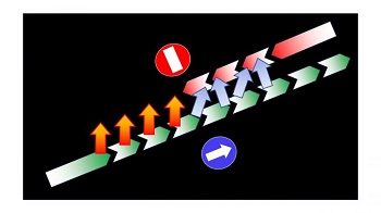
The spin is a type of angular momentum which is intrinsic to particles, grosso modo as if they were spinning on themselves. Particles can exchange their spin, and in this way spin currents can be formed in a material. Through years of research, scientists have learned how to control such spin currents in an analogous way such that they can control the flow of electrons, a field of physics known as spintronics.
The study of the effect of strong interactions in quantum systems is particularly challenging, however, it is well known that strong interaction between quantum particles can completely change the properties of a system, making it, for instance, ferromagnetic, superconducting, etc. Strong interactions in spin systems can also allow for the generation of interesting transport properties in a material.
Researchers from Singapore University of Technology and Design (SUTD), University Insubria and Universidade Federal de Minas Gerais have shown a completely new approach to controlling spin currents based on strong spin-spin interactions, which results in diodes for spin current with a giant rectification. In this work the researchers demonstrated, both analytically and using advanced numerical simulations that, if the interactions are stronger than a certain magnitude the system can drastically change and becomes an insulator, preventing currents from flowing. Interestingly, this drastic change to insulating behaviour only occurs when trying to impose the current in one direction. When trying to drive a spin current in the opposite direction, the flow is possible and the system is not an insulator.
These predictions, once tested in experiments with atoms near absolute zero temperature or with structures made of a few atoms deposited carefully on surfaces, can open the way to substantial progress in material science, and new devices can be built based on this principle.
SUTD Assistant Professor D. Poletti, who led the research effort, states that: "This is a very interesting effect we have stumbled upon. Much more interesting physics is yet to be uncovered in strongly interacting spintronic systems, and this can lead to the creation of new technologies."
Share on:


Testimonial
"The I-Connect007 team is outstanding—kind, responsive, and a true marketing partner. Their design team created fresh, eye-catching ads, and their editorial support polished our content to let our brand shine. Thank you all! "
Sweeney Ng - CEE PCBSuggested Items
I-Connect007 Launches Advanced Electronics Packaging Digest
09/15/2025 | I-Connect007I-Connect007 is pleased to announce the launch of Advanced Electronics Packaging Digest (AEPD), a new monthly digital newsletter dedicated to one of the most critical and rapidly evolving areas of electronics manufacturing: advanced packaging at the interconnect level.
VIDEOTON EAS's Bulgarian Subsidiary Expands Into Automotive Products
09/15/2025 | VideotonVEAS Bulgaria, engaged in electronics manufacturing, has joined the ranks of VIDEOTON companies authorized to produce automotive products.
Variosystems Strengthens North American Presence with Southlake Relaunch 2025
09/15/2025 | VariosystemsVariosystems celebrated the relaunch of its U.S. facility in Southlake, Texas. After months of redesign and reorganization, the opening marked more than just the return to a modernized production site—it was a moment to reconnect with our teams, partners, and the local community.
Hanwha Aerospace to Collaborate with BAE Systems on Advanced Anti-jamming GPS for Guided Missiles
09/15/2025 | HanwhaHanwha Aerospace has signed a contract with BAE Systems to integrate next-generation, anti-jamming Global Positioning System (GPS) technology into Hanwha Aerospace’s Deep Strike Capability precision-guided weapon system.
EV Group Achieves Breakthrough in Hybrid Bonding Overlay Control for Chiplet Integration
09/12/2025 | EV GroupEV Group (EVG), a leading provider of innovative process solutions and expertise serving leading-edge and future semiconductor designs and chip integration schemes, today unveiled the EVG®40 D2W—the first dedicated die-to-wafer overlay metrology platform to deliver 100 percent die overlay measurement on 300-mm wafers at high precision and speeds needed for production environments. With up to 15X higher throughput than EVG’s industry benchmark EVG®40 NT2 system designed for hybrid wafer bonding metrology, the new EVG40 D2W enables chipmakers to verify die placement accuracy and take rapid corrective action, improving process control and yield in high-volume manufacturing (HVM).