


 Trouble in Your Tank: Implementing Direct Metallization in Advanced Substrate Packaging
 It’s Only Common Sense: Storytelling That Sells—Stop Pitching, Start Painting Pictures
 The Right Approach: Get Ready for ISO 9001 Version 6


Insulator-metal Transition at the Nanoscale
May 25, 2018 | ICFOEstimated reading time: 2 minutes
An international team of researchers is able to probe the insulator-conductor phase transition of materials at the nanoscale resolution. Controlling the flow of electrons within circuits is how electronic devices work. This is achieved through the appropriate choice of materials. Metals allow electrons to flow freely and insulators prevent conduction. In general, the electrical properties of a material are determined when the material is fabricated and cannot be changed afterwards without changing the material. However, there are materials that can exhibit metal or insulator behaviour depending on their temperature. Being able switch their properties, these materials could lead to a new generation of electronic devices.
Vanadium Dioxide (VO2) is one such material. It can switch from an insulating phase to a metallic phase just above room temperature, a feature exploited already for sensors. However, the reason why the properties of this material change so dramatically has been a matter of scientific debate for over 50 years.
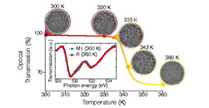
One of the challenges in understanding why and how this switch occurs is due to a process called phase separation. The insulator-metal phase transition is similar to the ice to liquid transition in water. When ice melts, both liquid and solid water can coexist in separate regions. Similarly, in VO2, insulating and metallic regions of the material can be coexisting at the same time during the transition. But unlike water, where the different regions are often large enough to see with the naked eye, in VO2 this separation occurs on the nanoscale and it is thus challenging to observe. As a result, it has been hard to know if the true properties of each phase, or the mixture of both phases, are being measured.
X-rays are a key tool for understanding the properties of materials, but it has been hard to use them to probe materials on the nanoscale because it is hard to build lenses for microscopes that can detect them. However, in a recent study published in Nano Letters, a team of researchers from ICFO and ALBA in Barcelona, the Technisch Universitat and Max-Born Institute in Berlin, and Vanderbilt University in Tennessee, has finally been able to probe the phase transitions that occur in thin films of Vanadium Dioxide (VO2) using resonant soft X-ray holography. This technique is capable of imaging the electronic and structural changes in this material with an unprecedented resolution at the nanoscale without the need of a len. By looking at the material with 50 nm resolution, the scientists were able to observe that defects in the material played an important role in initiating the phase transition from the insulator to the metal. However, more importantly, the authors also observed a third intermediate state formed during the phase transformation. Whilst some regions transformed directly from the insulating to metallic phase, others transformed into a second different insulating state before becoming metallic at higher temperatures with the exact pathway taken depending on the defects present in the material. The coexistences of three phases has radically changed the views of previous studies that assumed the presence of only two states during the transition. Even more, the study presents new ways in which the transition could be controlled.
In addition to the results obtained on the phase transition in VO2, the work also highlights the possibilities that X-ray holography can bring for studying materials on the nanoscale. The technique is the only method that can image real-time nanoscale dynamics and is now being used to study the properties of other intriguing materials such as high temperature superconductors.
Share on:


Testimonial
"The I-Connect007 team is outstanding—kind, responsive, and a true marketing partner. Their design team created fresh, eye-catching ads, and their editorial support polished our content to let our brand shine. Thank you all! "
Sweeney Ng - CEE PCBSuggested Items
I-Connect007 Launches Advanced Electronics Packaging Digest
09/15/2025 | I-Connect007I-Connect007 is pleased to announce the launch of Advanced Electronics Packaging Digest (AEPD), a new monthly digital newsletter dedicated to one of the most critical and rapidly evolving areas of electronics manufacturing: advanced packaging at the interconnect level.
Panasonic Industry will Double the Production Capacity of MEGTRON Multi-layer Circuit Board Materials Over the Next Five Years
09/15/2025 | Panasonic Industry Co., Ltd.Panasonic Industry Co., Ltd., a Panasonic Group company, announced plans for a major expansion of its global production capacity for MEGTRON multi-layer circuit board materials today. The company plans to double its production over the next five years to meet growing demand in the AI server and ICT infrastructure markets.
Trouble in Your Tank: Implementing Direct Metallization in Advanced Substrate Packaging
09/15/2025 | Michael Carano -- Column: Trouble in Your TankDirect metallization systems based on conductive graphite are gaining popularity throughout the world. The environmental and productivity gains achievable with this process are outstanding. Direct metallization reduces the costs of compliance, waste treatment, and legal issues related to chemical exposure. A graphite-based direct plate system has been devised to address these needs.
Fresh PCB Concepts: Designing for Success at the Rigid-flex Transition Area
08/28/2025 | Team NCAB -- Column: Fresh PCB ConceptsRigid-flex PCBs come in all shapes and sizes. Manufacturers typically use fire-retardant, grade 4 (FR-4) materials in the rigid section and flexible polyimide materials in the flex region. Because of the small size, some rigid-flex PCBs, like those for hearing aid devices, are among the most challenging to manufacture. However, regardless of its size, we should not neglect the transition area between the rigid and flexible material.
Global Sourcing Spotlight: How to Evaluate Supplier Capabilities Worldwide
08/20/2025 | Bob Duke -- Column: Global Sourcing SpotlightIn global sourcing, the difference between a competitive edge and a catastrophic disruption often comes down to how well you vet your suppliers. Sourcing advanced PCBs, precision components, or materials for complex assemblies demands diligence, skepticism, and more than a little time on airplanes. Here’s how to do your due diligence when evaluating international suppliers and why cutting corners can cost you more than money.