


 Trouble in Your Tank: Implementing Direct Metallization in Advanced Substrate Packaging
 It’s Only Common Sense: Storytelling That Sells—Stop Pitching, Start Painting Pictures
 The Right Approach: Get Ready for ISO 9001 Version 6


Rare Element to Provide Better Material for High-Speed Electronics
May 28, 2018 | Purdue UniversityEstimated reading time: 2 minutes
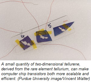
Purdue researchers have discovered a new two-dimensional material, derived from the rare element tellurium, to make transistors that carry a current better throughout a computer chip.
The discovery adds to a list of extremely thin, two-dimensional materials that engineers have tried to use for improving the operation speed of a chip’s transistors, which then allows information to be processed faster in electronic devices, such as phones and computers, and defense technologies like infrared sensors.
Other two-dimensional materials, such as graphene, black phosphorus and silicene, have lacked either stability at room temperature or the feasible production approaches required to nanomanufacture effective transistors for higher speed devices.
“All transistors need to send a large current, which translates to high-speed electronics,” said Peide Ye, Purdue’s Richard J. and Mary Jo Schwartz Professor of Electrical and Computer Engineering. “One-dimensional wires that currently make up transistors have very small cross sections. But a two-dimensional material, acting like a sheet, can send a current over a wider surface area.”
Tellurene, a two-dimensional film researchers found in the element tellurium, achieves a stable, sheet-like transistor structure with faster-moving “carriers” – meaning electrons and the holes they leave in their place. Despite tellurium’s rarity, the pros of tellurene would make transistors made from two-dimensional materials easier to produce on a larger scale. The researchers detail their findings in Nature Electronics.
“Even though tellurium is not abundant on the Earth’s crust, we only need a little bit to be synthesized through a solution method. And within the same batch, we have a very high production yield of two-dimensional tellurene materials,” said Wenzhuo Wu, assistant professor in Purdue’s School of Industrial Engineering. “You simply scale up the container that holds the solution, so productivity is high.”
Since electronics are typically in use at room temperature, naturally stable tellurene transistors at this temperature are more practical and cost-effective than other two-dimensional materials that have required a vacuum chamber or low operation temperature to achieve similar stability and performance.
The larger crystal flakes of tellurene also mean less barriers between flakes to electron movement – an issue with the more numerous, smaller flakes of other two-dimensional materials.
“High carrier mobility at room temperature means more practical applications,” Ye said. Faster-moving electrons and holes then lead to higher currents across a chip.
The researchers anticipate that because tellurene can grow on its own without the help of any other substance, the material could possibly find use in other applications beyond computer chip transistors, such as flexible printed devices that convert mechanical vibrations or heat to electricity.
“Tellurene is a multifunctional material, and Purdue is the birthplace for this new material,” Wu said. “In our opinion, this is much closer to the scalable production of two-dimensional materials with controlled properties for practical technologies.”
Wu and Ye’s work was supported by Purdue’s College of Engineering and School of Industrial Engineering, the National Science Foundation, Oak Ridge Associated Universities, the Air Force Office of Scientific Research, the Army Research Office and the Semiconductor Research Corporation. Collaborating paper authors received various funding from fellowships and grants.
Share on:


Testimonial
"We’re proud to call I-Connect007 a trusted partner. Their innovative approach and industry insight made our podcast collaboration a success by connecting us with the right audience and delivering real results."
Julia McCaffrey - NCAB GroupSuggested Items
I-Connect007 Launches Advanced Electronics Packaging Digest
09/15/2025 | I-Connect007I-Connect007 is pleased to announce the launch of Advanced Electronics Packaging Digest (AEPD), a new monthly digital newsletter dedicated to one of the most critical and rapidly evolving areas of electronics manufacturing: advanced packaging at the interconnect level.
Panasonic Industry will Double the Production Capacity of MEGTRON Multi-layer Circuit Board Materials Over the Next Five Years
09/15/2025 | Panasonic Industry Co., Ltd.Panasonic Industry Co., Ltd., a Panasonic Group company, announced plans for a major expansion of its global production capacity for MEGTRON multi-layer circuit board materials today. The company plans to double its production over the next five years to meet growing demand in the AI server and ICT infrastructure markets.
Trouble in Your Tank: Implementing Direct Metallization in Advanced Substrate Packaging
09/15/2025 | Michael Carano -- Column: Trouble in Your TankDirect metallization systems based on conductive graphite are gaining popularity throughout the world. The environmental and productivity gains achievable with this process are outstanding. Direct metallization reduces the costs of compliance, waste treatment, and legal issues related to chemical exposure. A graphite-based direct plate system has been devised to address these needs.
Fresh PCB Concepts: Designing for Success at the Rigid-flex Transition Area
08/28/2025 | Team NCAB -- Column: Fresh PCB ConceptsRigid-flex PCBs come in all shapes and sizes. Manufacturers typically use fire-retardant, grade 4 (FR-4) materials in the rigid section and flexible polyimide materials in the flex region. Because of the small size, some rigid-flex PCBs, like those for hearing aid devices, are among the most challenging to manufacture. However, regardless of its size, we should not neglect the transition area between the rigid and flexible material.
Global Sourcing Spotlight: How to Evaluate Supplier Capabilities Worldwide
08/20/2025 | Bob Duke -- Column: Global Sourcing SpotlightIn global sourcing, the difference between a competitive edge and a catastrophic disruption often comes down to how well you vet your suppliers. Sourcing advanced PCBs, precision components, or materials for complex assemblies demands diligence, skepticism, and more than a little time on airplanes. Here’s how to do your due diligence when evaluating international suppliers and why cutting corners can cost you more than money.