


 Trouble in Your Tank: Implementing Direct Metallization in Advanced Substrate Packaging
 It’s Only Common Sense: Storytelling That Sells—Stop Pitching, Start Painting Pictures
 The Right Approach: Get Ready for ISO 9001 Version 6


Researchers Explore New Applications for 'Smart' Material
May 30, 2018 | University of LuxembourgEstimated reading time: 2 minutes
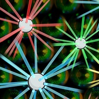
Research led by scientists from the University of Luxembourg has shown the potential of liquid crystal shells as enabling material for a vast array of future applications, ranging from autonomous driving to anti-counterfeiting technology and a new class of sensors.
Liquid Crystals, already widely used in flat-screen TVs, are materials that are in a state between solid and liquid. Prof. Jan Lagerwall and his team at the Physics and Materials Science Research Unit (PHYMS) at the University of Luxembourg have been investigating the unique mechanical and optical properties of microscopic shells that are produced of liquid crystal for several years. Now, in a multidisciplinary collaboration with IT scientists Dr Gabriele Lenzini and Prof. Peter Ryan of the University’s Interdisciplinary Center for Security and Trust (SnT) as well as Mathew Schwartz, Assistant Professor at the New Jersey Institute of Technology, they published a report in the scientific journal Advanced Materials describing potentially groundbreaking future applications for the material.
Guiding autonomous vehicles
Liquid Crystal shells, only fractions of a millimeter in size so they can easily be applied to surfaces, have several unique properties that could be utilised in engineering: As they reflect light highly selectively, they can be arranged into patterns that are readable for machines, akin to a QR code, adding coded information to objects. “These patterns could be used to guide autonomous vehicles or to instruct robots when handling workpieces in a factory. This could become important especially in indoors applications where GPS devices don’t work,” Prof. Lagerwall explains.
The shells can be manufactured to reflect only certain wavelengths of light, such as infrared, that would be invisible to the human eye. As the Liquid Crystal shells reflect light “omnidirectionally” meaning that beholders see the same pattern regardless of their position and viewing angle, the patterns can even be read by moving objects.
Tactile feeling for robots
Additionally, the shells can be manufactured in a way that they change their structure when they are exposed to certain external impacts, such as pressure, heat or specific chemicals. Together with computers to interpret these changes, the shells could be used as sensors, for example as pressure sensors in the fingertips of robots enabling tactile feeling which is currently hard to achieve in robotic engineering. Another application could be fire exit signage on walls inside buildings that only becomes visible when the temperature exceeds a certain threshold. The big advantage of these sensors is that they passively react to external impacts and don’t need electricity and batteries.
Preventing counterfeiting
Finally, liquid crystal shells could be used to prevent counterfeiting. The micropatterns that emerge when the shells are brought together are unique and impossible to copy. These unclonable patterns could be used to create uncopiable identifiers that can be attached to valuable objects, such as art works or expensive pharmaceuticals. In combination with cryptographic tools they could be used to create a system that ensures that a buyer or user has the original and not a counterfeited product.
Prof. Lagerwall makes clear that the ideas outlined in the report require further research. “Our hope is that the article can stimulate future research on liquid crystalline materials into new directions that are in line with the current societal developments,” he said.
Share on:


Testimonial
"Our marketing partnership with I-Connect007 is already delivering. Just a day after our press release went live, we received a direct inquiry about our updated products!"
Rachael Temple - AlltematedSuggested Items
I-Connect007 Launches Advanced Electronics Packaging Digest
09/15/2025 | I-Connect007I-Connect007 is pleased to announce the launch of Advanced Electronics Packaging Digest (AEPD), a new monthly digital newsletter dedicated to one of the most critical and rapidly evolving areas of electronics manufacturing: advanced packaging at the interconnect level.
Panasonic Industry will Double the Production Capacity of MEGTRON Multi-layer Circuit Board Materials Over the Next Five Years
09/15/2025 | Panasonic Industry Co., Ltd.Panasonic Industry Co., Ltd., a Panasonic Group company, announced plans for a major expansion of its global production capacity for MEGTRON multi-layer circuit board materials today. The company plans to double its production over the next five years to meet growing demand in the AI server and ICT infrastructure markets.
Trouble in Your Tank: Implementing Direct Metallization in Advanced Substrate Packaging
09/15/2025 | Michael Carano -- Column: Trouble in Your TankDirect metallization systems based on conductive graphite are gaining popularity throughout the world. The environmental and productivity gains achievable with this process are outstanding. Direct metallization reduces the costs of compliance, waste treatment, and legal issues related to chemical exposure. A graphite-based direct plate system has been devised to address these needs.
Fresh PCB Concepts: Designing for Success at the Rigid-flex Transition Area
08/28/2025 | Team NCAB -- Column: Fresh PCB ConceptsRigid-flex PCBs come in all shapes and sizes. Manufacturers typically use fire-retardant, grade 4 (FR-4) materials in the rigid section and flexible polyimide materials in the flex region. Because of the small size, some rigid-flex PCBs, like those for hearing aid devices, are among the most challenging to manufacture. However, regardless of its size, we should not neglect the transition area between the rigid and flexible material.
Global Sourcing Spotlight: How to Evaluate Supplier Capabilities Worldwide
08/20/2025 | Bob Duke -- Column: Global Sourcing SpotlightIn global sourcing, the difference between a competitive edge and a catastrophic disruption often comes down to how well you vet your suppliers. Sourcing advanced PCBs, precision components, or materials for complex assemblies demands diligence, skepticism, and more than a little time on airplanes. Here’s how to do your due diligence when evaluating international suppliers and why cutting corners can cost you more than money.