


 Trouble in Your Tank: Implementing Direct Metallization in Advanced Substrate Packaging
 It’s Only Common Sense: Storytelling That Sells—Stop Pitching, Start Painting Pictures
 The Right Approach: Get Ready for ISO 9001 Version 6


Building Nanomaterials for Next-Generation Computing
May 31, 2018 | AMERICAN INSTITUTE OF PHYSICSEstimated reading time: 2 minutes
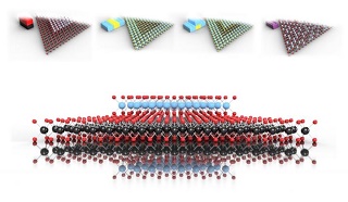
Nanoscientists at Northwestern University have developed a blueprint to fabricate new heterostructures from different types of 2-D materials. 2-D materials are single atom layers that can be stacked together like "nano-interlocking building blocks." Materials scientists and physicists are excited about the properties of 2-D materials and their potential applications. The researchers describe their blueprint in the Journal of Applied Physics, from AIP Publishing.
"We've outlined an easy, deterministic and readily deployable way to stack and stitch these individual layers into orders not seen in nature," said Jeffrey Cain, an author on the paper who was formerly at Northwestern University but is now at Lawrence Berkeley National Laboratory and the University of California.
Cain explained that for nanoscientists, "the dream" is to combine 2-D materials in any order and collate a library of these heterostructures with their documented properties. Scientists can then select appropriate heterostructures from the library for their desired applications. For instance, the computer industry is trying to make transistors smaller and faster to increase computing power. A nanoscale semiconductor with favorable electronic properties could be used to make transistors in next-generation computers.
So far, nanoscientists have lacked clear methods for fabricating heterostructures, and have not yet been able to develop this library. In this work, the scientists looked to solve these fabrication issues. After identifying trends in the literature, they tested different conditions to map out the different parameters required to grow specific heterostructures from four types of 2-D materials: molybdenum disulfide and diselenide, and tungsten disulfide and diselenide. To fully characterize the atomically thin final products, the scientists used microscopy and spectrometry techniques.
The group was inspired by the science of time-temperature-transformation diagrams in classical materials, which maps out heating and cooling profiles to generate precise metallic microstructures. Based on this method, the researchers packaged their findings into one diagrammatic technique -- the Time-Temperature-Architecture Diagram.
"People had previously written papers for specific morphologies, but we have unified it all and enabled the generation of these morphologies with one technique," Cain said.
The unified Time-Temperature-Architecture Diagrams provide directions for the exact conditions required to generate numerous heterostructure morphologies and compositions. Using these diagrams, the researchers developed a unique library of nanostructures with physical properties of interest to physicists and materials scientists. The Northwestern University scientists are now examining the behaviors displayed by some materials in their library, like the electron flow across the stitched junctions between materials.
The researchers hope that their blueprint design will be useful for heterostructure fabrication beyond the first four materials. "Our specific diagrams would need revisions in the context of each new material, but we think that this idea is applicable and extendable to other material systems," Cain said.
Share on:


Testimonial
"In a year when every marketing dollar mattered, I chose to keep I-Connect007 in our 2025 plan. Their commitment to high-quality, insightful content aligns with Koh Young’s values and helps readers navigate a changing industry. "
Brent Fischthal - Koh YoungSuggested Items
I-Connect007 Launches Advanced Electronics Packaging Digest
09/15/2025 | I-Connect007I-Connect007 is pleased to announce the launch of Advanced Electronics Packaging Digest (AEPD), a new monthly digital newsletter dedicated to one of the most critical and rapidly evolving areas of electronics manufacturing: advanced packaging at the interconnect level.
Panasonic Industry will Double the Production Capacity of MEGTRON Multi-layer Circuit Board Materials Over the Next Five Years
09/15/2025 | Panasonic Industry Co., Ltd.Panasonic Industry Co., Ltd., a Panasonic Group company, announced plans for a major expansion of its global production capacity for MEGTRON multi-layer circuit board materials today. The company plans to double its production over the next five years to meet growing demand in the AI server and ICT infrastructure markets.
Trouble in Your Tank: Implementing Direct Metallization in Advanced Substrate Packaging
09/15/2025 | Michael Carano -- Column: Trouble in Your TankDirect metallization systems based on conductive graphite are gaining popularity throughout the world. The environmental and productivity gains achievable with this process are outstanding. Direct metallization reduces the costs of compliance, waste treatment, and legal issues related to chemical exposure. A graphite-based direct plate system has been devised to address these needs.
Fresh PCB Concepts: Designing for Success at the Rigid-flex Transition Area
08/28/2025 | Team NCAB -- Column: Fresh PCB ConceptsRigid-flex PCBs come in all shapes and sizes. Manufacturers typically use fire-retardant, grade 4 (FR-4) materials in the rigid section and flexible polyimide materials in the flex region. Because of the small size, some rigid-flex PCBs, like those for hearing aid devices, are among the most challenging to manufacture. However, regardless of its size, we should not neglect the transition area between the rigid and flexible material.
Global Sourcing Spotlight: How to Evaluate Supplier Capabilities Worldwide
08/20/2025 | Bob Duke -- Column: Global Sourcing SpotlightIn global sourcing, the difference between a competitive edge and a catastrophic disruption often comes down to how well you vet your suppliers. Sourcing advanced PCBs, precision components, or materials for complex assemblies demands diligence, skepticism, and more than a little time on airplanes. Here’s how to do your due diligence when evaluating international suppliers and why cutting corners can cost you more than money.