


 Trouble in Your Tank: Implementing Direct Metallization in Advanced Substrate Packaging
 It’s Only Common Sense: Storytelling That Sells—Stop Pitching, Start Painting Pictures
 The Right Approach: Get Ready for ISO 9001 Version 6


Atomically Thin Nanowires Convert Heat to Electricity More Efficiently
June 1, 2018 | University of WarwickEstimated reading time: 1 minute
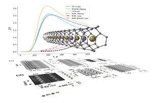
Waste heat can be converted to electricity more efficiently using one-dimensional nanoscale materials as thin as an atom – ushering a new way of generating sustainable energy – thanks to new research by the University of Warwick.
Led by Drs Andrij Vasylenko, Samuel Marks, Jeremy Sloan and David Quigley from Warwick’s Department of Physics, in collaboration with the Universities of Cambridge and Birmingham, the researchers have found that the most effective thermoelectric materials can be realised by shaping them into the thinnest possible nanowires.
Thermoelectric materials harvest waste heat and convert it into electricity - and are much sought-after as a renewable and environmentally friendly sources of energy.
Dr Andrij Vasylenko, from the University of Warwick’s Department of Physics and the paper’s first author, commented:
“In contrast to 3-dimensional material, isolated nanowires conduct less heat and more electricity at the same time. These unique properties yield unprecedented efficiency of heat-to-electricity conversion in one-dimensional materials.”
The researchers - which included the group of Dr Andrew J. Morris from the University of Birmingham - were investigating the crystallisation of tin telluride in extremely narrow carbon nanotubes used as templates for the formation of these materials in their lowest dimensional form.
In a combined theoretical-experimental research, they were able not only to establish a direct dependence between the size of a template and a resulting structure of a nanowire, but also to demonstrate how this technique can be used for regulation of the thermoelectric efficiency of tin telluride formed into nanowires 1-2 atoms in diameter.
First author Dr Vasylenko is excited about what this research could lead to:
“This opens up an opportunity for creation of a new generation of thermoelectric generators, but also for exploration of alternative candidate materials for thermoelectrics among abundant and non-toxic chemical elements.”
With a growing demand for both miniatuarisation and enhanced efficiency of thermoelectrics, nanostructuring offers a viable route for targeting both objectives.
Share on:


Testimonial
"In a year when every marketing dollar mattered, I chose to keep I-Connect007 in our 2025 plan. Their commitment to high-quality, insightful content aligns with Koh Young’s values and helps readers navigate a changing industry. "
Brent Fischthal - Koh YoungSuggested Items
I-Connect007 Launches Advanced Electronics Packaging Digest
09/15/2025 | I-Connect007I-Connect007 is pleased to announce the launch of Advanced Electronics Packaging Digest (AEPD), a new monthly digital newsletter dedicated to one of the most critical and rapidly evolving areas of electronics manufacturing: advanced packaging at the interconnect level.
Panasonic Industry will Double the Production Capacity of MEGTRON Multi-layer Circuit Board Materials Over the Next Five Years
09/15/2025 | Panasonic Industry Co., Ltd.Panasonic Industry Co., Ltd., a Panasonic Group company, announced plans for a major expansion of its global production capacity for MEGTRON multi-layer circuit board materials today. The company plans to double its production over the next five years to meet growing demand in the AI server and ICT infrastructure markets.
Trouble in Your Tank: Implementing Direct Metallization in Advanced Substrate Packaging
09/15/2025 | Michael Carano -- Column: Trouble in Your TankDirect metallization systems based on conductive graphite are gaining popularity throughout the world. The environmental and productivity gains achievable with this process are outstanding. Direct metallization reduces the costs of compliance, waste treatment, and legal issues related to chemical exposure. A graphite-based direct plate system has been devised to address these needs.
Fresh PCB Concepts: Designing for Success at the Rigid-flex Transition Area
08/28/2025 | Team NCAB -- Column: Fresh PCB ConceptsRigid-flex PCBs come in all shapes and sizes. Manufacturers typically use fire-retardant, grade 4 (FR-4) materials in the rigid section and flexible polyimide materials in the flex region. Because of the small size, some rigid-flex PCBs, like those for hearing aid devices, are among the most challenging to manufacture. However, regardless of its size, we should not neglect the transition area between the rigid and flexible material.
Global Sourcing Spotlight: How to Evaluate Supplier Capabilities Worldwide
08/20/2025 | Bob Duke -- Column: Global Sourcing SpotlightIn global sourcing, the difference between a competitive edge and a catastrophic disruption often comes down to how well you vet your suppliers. Sourcing advanced PCBs, precision components, or materials for complex assemblies demands diligence, skepticism, and more than a little time on airplanes. Here’s how to do your due diligence when evaluating international suppliers and why cutting corners can cost you more than money.