


 Global PCB Connections: Rigid-flex and Flexible PCBs—The Backbone of Modern Electronics
 Flexible Thinking: The Key to a Successful Flex Circuit Design Transfer
 Happy’s Tech Talk #29: Bend-to-Install Semi-flex FR-4


Designer Materials with Completely Random Structures Might Enable Quantum Computing
June 5, 2018 | Aalto UniversityEstimated reading time: 1 minute
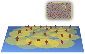
Designing quantum materials with exotic and unprecedented electrical properties has the field of physics teeming with buzz. Researchers at Aalto University in Finland have now introduced a significant turn in this discussion by developing an amorphous material which exhibits topological superconductivity. Until this point, these materials have required highly regular structures to show desired electrical properties.
The findings, published in Nature Communications, bring the field one step closer to application. Topological superconductors and insulators are considered to be possible building blocks of lossless components for quantum computers. While topological superconductors might not exist in nature, they can be fabricated, as the study demonstrates.
‘We have presented a method of fabricating topological materials in amorphous systems with randomly placed constituents. This means we can achieve superconductivity in the material by sprinkling magnetic atoms on a superconducting surface completely at random, not in highly-defined and ornamented lattices, for example,’ explains doctoral student Kim Pöyhönen.
The recent boom on topological superconductors stems mainly from an unconventional quantum-level phenomenon, a collective movement of many individual particles called Majorana fermion excitations. They have been envisioned as critical ingredients of topological quantum computers.
‘Getting highly irregular, random systems to work as topological superconductors will potentially make their fabrication and manufacture much more convenient compared to current methods,’ says research group leader, Docent Teemu Ojanen.
Perhaps for now, the implications of the random quantum material verge only on fundamental research, but that might not be the case for much longer.
‘For topological quantum matter to find its way to actual applications, it’s imperative we find even more new candidates for amorphous topological materials,’ states Ojanen.
Share on:


Testimonial
"Your magazines are a great platform for people to exchange knowledge. Thank you for the work that you do."
Simon Khesin - Schmoll MaschinenSuggested Items
Sealed for Survival: Potting Electronics for the Toughest Environments
10/29/2025 | Beth Massey, MacDermid Alpha Electronics SolutionsElectronics deployed in harsh conditions face relentless threats from vibration, impact, chemical contaminants, airborne pollutants, and moisture, conditions that can quickly lead to failure without robust protection. Potting, the process of encapsulating electronics in a protective polymer, is a widely used strategy to safeguard devices from both environmental and mechanical hazards.
Driving Innovation: Mechanical and Optical Processes During Rigid-flex Production
10/28/2025 | Kurt Palmer -- Column: Driving InnovationRigid-flex printed circuit boards are a highly effective solution for placing complex circuitry in tight, three-dimensional spaces. They are now indispensable across a range of industries, from medical devices and aerospace to advanced consumer electronics, helping designers make the most efficient use of available space. However, their unique construction—combining rigid and flexible materials—presents a fundamental challenge for PCB manufacturers.
SMTAI 2025 Review: Reflecting on a Pragmatic and Forward-looking Industry
10/27/2025 | Marcy LaRont, I-Connect007Leaving the show floor on the final afternoon of SMTA International last week in Rosemont, Illinois, it was clear that the show remains a grounded, technically driven event that delivers a solid program, good networking, and an easy space to commune with industry colleagues and meet with customers.
ITW EAE Despatch Ovens Now Support ASTM 5423 Testing
10/15/2025 | ITW EAEAs the demand for high-performance electrical insulation materials continues to grow—driven by the rapid expansion of electric vehicles (EVs) and energy storage systems—thermal processing has become a critical step in material development.
Beyond Thermal Conductivity: Exploring Polymer-based TIM Strategies for High-power-density Electronics
10/13/2025 | Padmanabha Shakthivelu and Nico Bruijnis, MacDermid Alpha Electronics SolutionsAs power density and thermal loads continue to increase, effective thermal management becomes increasingly important. Rapid and efficient heat transfer from power semiconductor chip packages is essential for achieving optimal performance and ensuring long-term reliability of temperature-sensitive components. This is particularly crucial in power systems that support advanced applications such as green energy generation, electric vehicles, aerospace, and defense, along with high-speed computing for data centers and artificial intelligence (AI).