


 Trouble in Your Tank: Implementing Direct Metallization in Advanced Substrate Packaging
 It’s Only Common Sense: Storytelling That Sells—Stop Pitching, Start Painting Pictures
 The Right Approach: Get Ready for ISO 9001 Version 6


A New Type of Optical Ceramic Material
June 7, 2018 | Far Eastern Federal UniversityEstimated reading time: 2 minutes
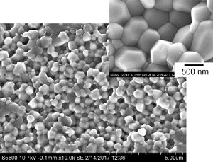
Multilayer YAG/Nd3+:YAG/YAG composite laser ceramics with a high concentration of active additive outclassed the commercial glass and single crystals used in laser technologies by it's physical and mechanical characteristics. The slope efficiency of the new one is at least twice as the existed materials have got.
The new type of optical ceramics was designed by young scientists' team of the Far Eastern Federal University (FEFU) under Denis Yu. Kosyanov, Ph.D., senior researcher of the School of Natural Sciences (FEFU). The scientific and technical results of the work presented for publishing in the Ceramics International. Patent application was filed to RosPatent (reg.number 2018119380).
Ceramics created is one of the numbers of other results of the work to design transparent polycrystalline materials with specified properties. The results of previous research have already been published in high-ranking scientific journals Journal of Alloys and Compounds, Journal of the European Ceramic Society, Ceramics International, Optical Materials, etc.
'The new so-called 'fine-grained' ceramics YAG: Nd contains up to 4 at.% active additive of neodymium ions. So far, that is unattainable with modern technologies of laser crystals production. The applying of the innovative method of reaction spark plasma sintering (RSPS) made it possible to carry out the synthesis 10-20 times faster comparing to the known approaches, and to obtain a monophase polycrystal with an average grain size of 500 nm', senior researcher Denis Kasyanov comments on. 'An important result of the invention is the simplification and cost reduction of the technology of obtaining optical materials with a YAG structure. In particular, the easiness of controlling the variety and the amount of active additive within the RSPS method makes it possible to vary the functionality of the final material', he proceeds.
The research was carried out as a part of the project of the Ministry of Education and Science of the Russian Federation (Project No. 3.2168.2017/4.6), and to increase the competitiveness of the FEFU which became one of the fourteen Russian Universities participating in the project '5-100' since 2014.
The researching direction of the team led by Denis Kosyanov is considering as promising. There are a number of problems established in front of scientists to further research. To gain success in solving them FEFU designed the curriculum for magistracy, postgraduate, and postdoctoral studies.
The 'New ceramic materials' is one of the main researching areas in the key laboratory 'Materials' established by FEFU. To ensure a breakthrough, we are already attracting Russian and foreign scientists from leading Universities and research organizations', Kirill Golokhvast tells, Ph.D., FEFU provost for science work. He also noticed that the team of the key laboratory will be formed of talented young physicists, biologists, and, of course, materials scientists.
Share on:


Testimonial
"Advertising in PCB007 Magazine has been a great way to showcase our bare board testers to the right audience. The I-Connect007 team makes the process smooth and professional. We’re proud to be featured in such a trusted publication."
Klaus Koziol - atgSuggested Items
I-Connect007 Launches Advanced Electronics Packaging Digest
09/15/2025 | I-Connect007I-Connect007 is pleased to announce the launch of Advanced Electronics Packaging Digest (AEPD), a new monthly digital newsletter dedicated to one of the most critical and rapidly evolving areas of electronics manufacturing: advanced packaging at the interconnect level.
Panasonic Industry will Double the Production Capacity of MEGTRON Multi-layer Circuit Board Materials Over the Next Five Years
09/15/2025 | Panasonic Industry Co., Ltd.Panasonic Industry Co., Ltd., a Panasonic Group company, announced plans for a major expansion of its global production capacity for MEGTRON multi-layer circuit board materials today. The company plans to double its production over the next five years to meet growing demand in the AI server and ICT infrastructure markets.
Trouble in Your Tank: Implementing Direct Metallization in Advanced Substrate Packaging
09/15/2025 | Michael Carano -- Column: Trouble in Your TankDirect metallization systems based on conductive graphite are gaining popularity throughout the world. The environmental and productivity gains achievable with this process are outstanding. Direct metallization reduces the costs of compliance, waste treatment, and legal issues related to chemical exposure. A graphite-based direct plate system has been devised to address these needs.
Fresh PCB Concepts: Designing for Success at the Rigid-flex Transition Area
08/28/2025 | Team NCAB -- Column: Fresh PCB ConceptsRigid-flex PCBs come in all shapes and sizes. Manufacturers typically use fire-retardant, grade 4 (FR-4) materials in the rigid section and flexible polyimide materials in the flex region. Because of the small size, some rigid-flex PCBs, like those for hearing aid devices, are among the most challenging to manufacture. However, regardless of its size, we should not neglect the transition area between the rigid and flexible material.
Global Sourcing Spotlight: How to Evaluate Supplier Capabilities Worldwide
08/20/2025 | Bob Duke -- Column: Global Sourcing SpotlightIn global sourcing, the difference between a competitive edge and a catastrophic disruption often comes down to how well you vet your suppliers. Sourcing advanced PCBs, precision components, or materials for complex assemblies demands diligence, skepticism, and more than a little time on airplanes. Here’s how to do your due diligence when evaluating international suppliers and why cutting corners can cost you more than money.