


 Trouble in Your Tank: Implementing Direct Metallization in Advanced Substrate Packaging
 It’s Only Common Sense: Storytelling That Sells—Stop Pitching, Start Painting Pictures
 The Right Approach: Get Ready for ISO 9001 Version 6


A Nanotech Sensor Turns Molecular Fingerprints into Bar Codes
June 8, 2018 | EPFLEstimated reading time: 2 minutes
A new system developed at EPFL can detect and analyze molecules with very high precision and without needing bulky equipment. It opens the door to large-scale, image-based detection of materials aided by artificial intelligence. The research has been published in Science.
Infrared spectroscopy is the benchmark method for detecting and analyzing organic compounds. But it requires complicated procedures and large, expensive instruments, making device miniaturization challenging and hindering its use for some industrial and medical applications and for data collection out in the field, such as for measuring pollutant concentrations. Furthermore, it is fundamentally limited by low sensitivities and therefore requires large sample amounts.
However, scientists at EPFL’s School of Engineering and at Australian National University (ANU) have developed a compact and sensitive nanophotonic system that can identify a molecule’s absorption characteristics without using conventional spectrometry. The scientists have already used their system to detect polymers, pesticides and organic compounds. What’s more, it is compatible with CMOS technology.
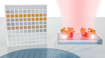
Their system consists of an engineered surface covered with hundreds of tiny sensors called metapixels, which can generate a distinct bar code for every molecule that the surface comes into contact with. These bar codes can be massively analyzed and classified using advanced pattern recognition and sorting technology such as artificial neural networks. This research—which sits at the crossroads of physics, nanotechnology and big data—has been published in Science.
Translating molecules into bar codes
The chemical bonds in organic molecules each have a specific orientation and vibrational mode. It influences the way molecules absorb light, giving each one a unique “signature.” Infrared spectroscopy detects whether a given molecule is present in a sample by seeing if the sample absorbs light rays at the molecule’s signature frequencies. However, such analyses require lab instruments with a hefty size and price tag.
The pioneering system developed by the EPFL scientists is both highly sensitive and capable of being miniaturized; it uses nanostructures that can trap light on the nanoscale and thereby provide very high detection levels for samples on the surface. “The molecules we want to detect are nanometric in scale, so bridging this size gap is an essential step,” says Hatice Altug, head of EPFL’s BioNanoPhotonic Systems Laboratory and a coauthor of the study.
The system’s nanostructures are grouped into what are called metapixels so that each one resonates at a different frequency. When a molecule comes into contact with the surface, the way the molecule absorbs light changes the behavior of all the metapixels it touches.
“Importantly, the metapixels are arranged in such a way that different vibrational frequencies are mapped to different areas on the surface,” says Andreas Tittl, lead author of the study.
This creates a pixelated map of light absorption that can be translated into a molecular bar code – all without using a spectrometer.
“Thanks to our sensors’ unique optical properties, we can generate bar codes even with broadband light sources and detectors,” says Aleksandrs Leitis, a coauthor of the study.
There are a number of potential applications for this new system. “For instance, it could be used to make portable medical testing devices that generate bar codes for each of the biomarkers found in a blood sample,” says Dragomir Neshev, another coauthor of the study.
Artificial intelligence could be used in conjunction with this new technology to create and process a whole library of molecular bar codes for compounds ranging from protein and DNA to pesticides and polymers. That would give researchers a new tool for quickly and accurately spotting miniscule amounts of compounds present in complex samples.
Share on:


Testimonial
"Our marketing partnership with I-Connect007 is already delivering. Just a day after our press release went live, we received a direct inquiry about our updated products!"
Rachael Temple - AlltematedSuggested Items
I-Connect007 Launches Advanced Electronics Packaging Digest
09/15/2025 | I-Connect007I-Connect007 is pleased to announce the launch of Advanced Electronics Packaging Digest (AEPD), a new monthly digital newsletter dedicated to one of the most critical and rapidly evolving areas of electronics manufacturing: advanced packaging at the interconnect level.
VIDEOTON EAS's Bulgarian Subsidiary Expands Into Automotive Products
09/15/2025 | VideotonVEAS Bulgaria, engaged in electronics manufacturing, has joined the ranks of VIDEOTON companies authorized to produce automotive products.
Variosystems Strengthens North American Presence with Southlake Relaunch 2025
09/15/2025 | VariosystemsVariosystems celebrated the relaunch of its U.S. facility in Southlake, Texas. After months of redesign and reorganization, the opening marked more than just the return to a modernized production site—it was a moment to reconnect with our teams, partners, and the local community.
Hanwha Aerospace to Collaborate with BAE Systems on Advanced Anti-jamming GPS for Guided Missiles
09/15/2025 | HanwhaHanwha Aerospace has signed a contract with BAE Systems to integrate next-generation, anti-jamming Global Positioning System (GPS) technology into Hanwha Aerospace’s Deep Strike Capability precision-guided weapon system.
EV Group Achieves Breakthrough in Hybrid Bonding Overlay Control for Chiplet Integration
09/12/2025 | EV GroupEV Group (EVG), a leading provider of innovative process solutions and expertise serving leading-edge and future semiconductor designs and chip integration schemes, today unveiled the EVG®40 D2W—the first dedicated die-to-wafer overlay metrology platform to deliver 100 percent die overlay measurement on 300-mm wafers at high precision and speeds needed for production environments. With up to 15X higher throughput than EVG’s industry benchmark EVG®40 NT2 system designed for hybrid wafer bonding metrology, the new EVG40 D2W enables chipmakers to verify die placement accuracy and take rapid corrective action, improving process control and yield in high-volume manufacturing (HVM).