


 Trouble in Your Tank: Implementing Direct Metallization in Advanced Substrate Packaging
 It’s Only Common Sense: Storytelling That Sells—Stop Pitching, Start Painting Pictures
 The Right Approach: Get Ready for ISO 9001 Version 6


Silicon-Perovskite Solar Cells Achieve Record Efficiency of 25.2%
June 12, 2018 | EPFLEstimated reading time: 3 minutes
In Neuchâtel (Switzerland), researchers from EPFL and CSEM have combined silicon- and perovskite-based solar cells. The resulting efficiency of 25.2% is a record for this type of tandem cell. Their innovative yet simple manufacturing technique could be directly integrated into existing production lines, and efficiency could eventually rise above 30%.
In the field of photovoltaic technologies, silicon-based solar cells make up 90% of the market. In terms of cost, stability and efficiency (20-22% for a typical solar cell on the market), they are well ahead of the competition.
However, after decades of research and investment, silicon-based solar cells are now close to their maximum theoretical efficiency. As a result, new concepts are required to achieve a long-term reduction in solar electricity prices and allow photovoltaic technology to become a more widely adopted way of generating power.
One solution is to place two different types of solar cells on top of each other to maximize the conversion of light rays into electrical power. These “double-junction” cells are being widely researched in the scientific community, but are expensive to make. Now research teams in Neuchâtel – from EPFL’s Photovoltaics Laboratory and the CSEM PV-center – have developed an economically competitive solution. They have integrated a perovskite cell directly on top of a standard silicon-based cell, obtaining a record efficiency of 25.2%. Their production method is promising, because it would add only a few extra steps to the current silicon-cell production process, and the cost would be reasonable. Their research has been published in Nature Materials.
Perovskite-on-silicon: a nanometric sandwich
Perovskite’s unique properties have prompted a great deal of research into its use in solar cells over the last few years. In the space of nine years, the efficiency of these cells has risen by a factor of six. Perovskite allows high conversion efficiency to be achieved at a potentially limited production cost.
In tandem cells, perovskite complements silicon: it converts blue and green light more efficiently, while silicon is better at converting red and infra-red light. “By combining the two materials, we can maximize the use of the solar spectrum and increase the amount of power generated. The calculations and work we have done show that a 30% efficiency should soon be possible,” say the study’s main authors Florent Sahli and Jérémie Werner.
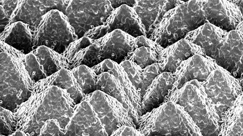
However, creating an effective tandem structure by superposing the two materials is no easy task. “Silicon’s surface consists of a series of pyramids measuring around 5 microns, which trap light and prevent it from being reflected. However, the surface texture makes it hard to deposit a homogeneous film of perovskite,” explains Quentin Jeangros, who co-authored the paper.
When the perovskite is deposited in liquid form, as it usually is, it accumulates in the valleys between the pyramids while leaving the peaks uncovered, leading to short circuits.
A key layer ensuring an optimal microstructure
Scientists at EPFL and CSEM have gotten around that problem by using evaporation methods to form an inorganic base layer that fully covers the pyramids. That layer is porous, enabling it to retain the liquid organic solution that is then added using a thin-film deposition technique called spin-coating. The researchers subsequently heat the substrate to a relatively low temperature of 150°C to crystallize a homogeneous film of perovskite on top of the silicon pyramids.
“Until now, the standard approach for making a perovskite/silicon tandem cell was to level off the pyramids of the silicon cell, which decreased its optical properties and therefore its performance, before depositing the perovskite cell on top of it. It also added steps to the manufacturing process,” says Florent Sahli.
Updating existing technologies
The new type of tandem cell is highly efficient and directly compatible with monocrystalline silicon-based technologies, which benefit from long-standing industrial expertise and are already being produced profitably. “We are proposing to use equipment that is already in use, just adding a few specific stages. Manufacturers won’t be adopting a whole new solar technology, but simply updating the production lines they are already using for silicon-based cells,” explains Christophe Ballif, head of EPFL’s Photovoltaics Laboratory and CSEM’s PV-Center.
At the moment, research is continuing in order to increase efficiency further and give the perovskite film more long-term stability. Although the team has made a breakthrough, there is still work to be done before their technology can be adopted commercially.
Share on:


Testimonial
"Our marketing partnership with I-Connect007 is already delivering. Just a day after our press release went live, we received a direct inquiry about our updated products!"
Rachael Temple - AlltematedSuggested Items
Panasonic Industry will Double the Production Capacity of MEGTRON Multi-layer Circuit Board Materials Over the Next Five Years
09/15/2025 | Panasonic Industry Co., Ltd.Panasonic Industry Co., Ltd., a Panasonic Group company, announced plans for a major expansion of its global production capacity for MEGTRON multi-layer circuit board materials today. The company plans to double its production over the next five years to meet growing demand in the AI server and ICT infrastructure markets.
VIDEOTON EAS's Bulgarian Subsidiary Expands Into Automotive Products
09/15/2025 | VideotonVEAS Bulgaria, engaged in electronics manufacturing, has joined the ranks of VIDEOTON companies authorized to produce automotive products.
Variosystems Strengthens North American Presence with Southlake Relaunch 2025
09/15/2025 | VariosystemsVariosystems celebrated the relaunch of its U.S. facility in Southlake, Texas. After months of redesign and reorganization, the opening marked more than just the return to a modernized production site—it was a moment to reconnect with our teams, partners, and the local community.
Integrating Uniplate PLBCu6 With the Digital Factory Suite
09/12/2025 | Giovanni Obino and Andreas Schatz, MKS' AtotechPrinted circuit board manufacturing is rapidly changing, driven by miniaturization, stringent reliability requirements, and growing pressure for sustainable production. Meeting these challenges requires more than incremental improvements; it demands a combination of precise equipment and real-time process intelligence. The pairing of Uniplate® PLBCu6 with the Digital Factory Suite (DFS) demonstrates how hardware and software can work together to create more responsive, resource-efficient manufacturing.
United Electronics Corporation Unveils Revolutionary CIMS Galaxy 30 Automated Optical Inspection System
09/11/2025 | United Electronics CorporationUnited Electronics Corporation (UEC) today announced the launch of its new groundbreaking CIMS Galaxy 30 Automated Optical Inspection (AOI) machine, setting a new industry standard for precision electronics manufacturing quality control. The Galaxy 30, developed and manufactured by CIMS, represents a significant leap forward in inspection technology, delivering exceptional speed improvements and introducing cutting-edge artificial intelligence capabilities.