


 Global PCB Connections: Rigid-flex and Flexible PCBs—The Backbone of Modern Electronics
 Flexible Thinking: The Key to a Successful Flex Circuit Design Transfer
 Happy’s Tech Talk #29: Bend-to-Install Semi-flex FR-4


Atotech to Introduce Cupracid Flex and InPro Flex
June 13, 2018 | AtotechEstimated reading time: 2 minutes
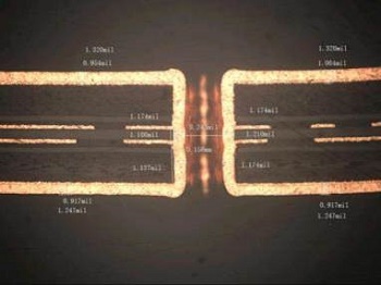
The flex/ flex-rigid PCB market continues to grow as more and more designs call for flexible inner layers with ever finer lines and spaces. At the same time, the need for high volume reel to reel formats as well as pattern plating with lower base copper thickness drives the FPCB market.
As one of the market leaders for BMV filling and through hole filling in the IC-substrate market, Atotech has developed two new acid copper processes – InPro Flex and Cupracid Flex – to serve the flexible printed circuit board market and support its customers to overcome the current technical barriers in FPCB manufacturing.
Excellent throwing power: Board thickness: 0.3mm, Hole: 0.15mm, CD: 2.8ASD, Line speed: 0.6m/min, Flow rate: 15HZ, Average TP% : 120%
Cupracid Flex and InPro Flex
“Cupracid Flex and InPro Flex are specifically designed for standard conformal flex and rigid-flex applications. While the Cupracid Flex process is for use in vertical systems with soluble anodes, InPro® Flex can be used in systems with insoluble anodes,” states Mustafa Oezkoek, Global Product Manager Panel and Pattern Plating at Atotech Deutschland GmbH.
The simple two additive processes can be analyzed by standard CVS method and are suitable for vertical equipment or vertical reel to reel equipment with educator or sparger systems. They can be operated in panel and pattern plating and provide excellent line shape, outstanding crystal structure and a ductility of more than 23% in either manufacturing method.
Features and Benefits
“Cupracid Flex and InPro Flex are highly reliable processes and deliver excellent physical properties,” continues Mustafa. “Both solutions assure first-rate throwing power at high current densities without any corner flattening. At the same time, pattern uniformity and line shape are very good. And, according to IPC, the bending performance is exceptional.”
Both products have been rolled out globally and are available worldwide.
About Atotech
Atotech is one of the world’s leading manufacturers of specialty chemicals and equipment for the printed circuit board, IC-substrate and semiconductor industries, as well as for the decorative and functional surface finishing industries. Atotech has annual sales of USD1.2 billion (2017). The company is fully committed to sustainability – we develop technologies to minimize waste and to reduce environmental impact. Atotech has its headquarters in Berlin, Germany, and employs about 4,000 people in over 40 countries. About a quarter of all staff works in one of the four locations in Germany: Berlin, Feucht, Neuruppin, and Trebur. For more information, click here.
Share on:


Testimonial
"Our marketing partnership with I-Connect007 is already delivering. Just a day after our press release went live, we received a direct inquiry about our updated products!"
Rachael Temple - AlltematedSuggested Items
Closing the Loop on PCB Etching Waste
09/09/2025 | Shawn Stone, IECAs the PCB industry continues its push toward greener, more cost-efficient operations, Sigma Engineering’s Mecer System offers a comprehensive solution to two of the industry’s most persistent pain points: etchant consumption and rinse water waste. Designed as a modular, fully automated platform, the Mecer System regenerates spent copper etchants—both alkaline and acidic—and simultaneously recycles rinse water, transforming a traditionally linear chemical process into a closed-loop system.
Driving Innovation: Depth Routing Processes—Achieving Unparalleled Precision in Complex PCBs
09/08/2025 | Kurt Palmer -- Column: Driving InnovationIn PCB manufacturing, the demand for increasingly complex and miniaturized designs continually pushes the boundaries of traditional fabrication methods, including depth routing. Success in these applications demands not only on robust machinery but also sophisticated control functions. PCB manufacturers rely on advanced machine features and process methodologies to meet their precise depth routing goals. Here, I’ll explore some crucial functions that empower manufacturers to master complex depth routing challenges.
Trouble in Your Tank: Minimizing Small-via Defects for High-reliability PCBs
08/27/2025 | Michael Carano -- Column: Trouble in Your TankTo quote the comedian Stephen Wright, “If at first you don’t succeed, then skydiving is not for you.” That can be the battle cry when you find that only small-diameter vias are exhibiting voids. Why are small holes more prone to voids than larger vias when processed through electroless copper? There are several reasons.
The Government Circuit: Navigating New Trade Headwinds and New Partnerships
08/25/2025 | Chris Mitchell -- Column: The Government CircuitAs global trade winds continue to howl, the electronics manufacturing industry finds itself at a critical juncture. After months of warnings, the U.S. Government has implemented a broad array of tariff increases, with fresh duties hitting copper-based products, semiconductors, and imports from many nations. On the positive side, tentative trade agreements with Europe, China, Japan, and other nations are providing at least some clarity and counterbalance.
How Good Design Enables Sustainable PCBs
08/21/2025 | Gerry Partida, Summit InterconnectSustainability has become a key focus for PCB companies seeking to reduce waste, conserve energy, and optimize resources. While many discussions on sustainability center around materials or energy-efficient processes, PCB design is an often overlooked factor that lies at the heart of manufacturing. Good design practices, especially those based on established IPC standards, play a central role in enabling sustainable PCB production. By ensuring designs are manufacturable and reliable, engineers can significantly reduce the environmental impact of their products.