


 Driving Innovation: Direct Imaging vs. Conventional Exposure
 It’s Only Common Sense: Selling to Today's Generation of Buyers
 Dan’s Biz Bookshelf: ‘Believe in Better'


Sculpting with Graphene Foam
June 15, 2018 | Rice UniversityEstimated reading time: 2 minutes
Rice University scientists have developed a simple way to produce conductive, three-dimensional objects made of graphene foam. The squishy solids look and feel something like a child’s toy but offer new possibilities for energy storage and flexible electronic sensor applications, according to Rice chemist James Tour.
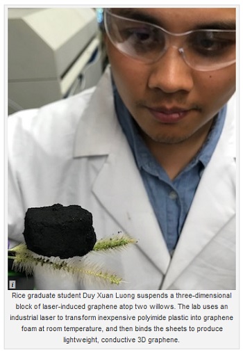
The technique detailed in Advanced Materials is an extension of groundbreaking work by the Tour lab that produced the first laser-induced graphene (LIG) in 2014 by heating inexpensive polyimide plastic sheets with a laser.
The laser burns halfway through the plastic and turns the top into interconnected flakes of 2D carbon that remain attached to the bottom half. LIG can be made in macroscale patterns at room temperature.
The lab extended its technique to create LIG on wood and even food, but 3D objects of pure graphene were less practical until now, Tour said.
“Now we have built a prototype machine that lets us make graphene foam into 3D objects through automated successive layering and laser exposure,” Tour said. “This truly brings graphene into the third dimension without furnaces or the need for metal catalysts, and our process is easily scaled.”
The new method is based on laminated object manufacturing, in which layers of a material are assembled and then cut to shape. In this case, the bottom LIG layer remains attached to its polyimide base. A second layer is coated with ethylene glycol and placed facedown on the first, like a jelly sandwich. Its polyimide top is then burned into graphene; the process is repeated until the block is complete.
The ethylene glycol binder is evaporated away on a hot plate, and any remaining polyimide can be removed in a furnace. That leaves a pristine, spongy carbon block, said Duy Xuan Luong, a Rice graduate student and co-lead author of the paper. The Rice lab stacked up to five layers of foam and then used a custom-built fiber lasing system on a modified 3D printer to mill the block into complex shapes.
The lab assembled proof-of-concept lithium-ion capacitors that used 3D LIG as both anodes and cathodes. The anode’s gravimetric capacity of 354 milliamp hours per gram neared the theoretical limit of graphite, while the cathode’s capacity exceeded the average capacity of other carbon materials. Full test cells retained about 70 percent of their capacity after 970 charge-discharge cycles.
“This is excellent performance in these new-generation lithium-ion capacitors, which capture the best properties of lithium-ion batteries and capacitor hybrids,” Tour said.
The researchers then infused a block of 3D LIG with liquid polydimethylsiloxane through its 20- to 30-nanometer pores. This created a stronger, still-flexible, conductive material without changing the original foam’s shape. From this material, they made a flexible sensor that accurately recorded the pulse from the wrist of a volunteer and said further calibration of the device would let them extract blood pressure from the pulse waveform.
Rice alumnus Ajay Subramanian is co-lead author of the paper. Co-authors are Rice graduate students Gladys Lopez Silva, Kaichun Yang, Peter Samora Owuor, Tuo Wang and Zhe Wang; former postdoctoral researcher Jongwon Yoon, now a senior researcher at the Korea Basic Science Institute; undergraduate Savannah Cofer; Jun Lou, a professor of materials science and nanoengineering; and Pulickel Ajayan, chair of Rice’s Department of Materials Science and NanoEngineering, the Benjamin M. and Mary Greenwood Anderson Professor in Engineering and a professor of chemistry.
The Air Force Office of Scientific Research and the Vietnam Education Foundation supported the research.
Share on:


Suggested Items
Indium Corporation Expert to Present on Automotive and Industrial Solder Bonding Solutions at Global Electronics Association Workshop
06/26/2025 | IndiumIndium Corporation Principal Engineer, Advanced Materials, Andy Mackie, Ph.D., MSc, will deliver a technical presentation on innovative solder bonding solutions for automotive and industrial applications at the Global Electronics A
Gorilla Circuits Elevates PCB Precision with Schmoll’s Optiflex II Alignment System
06/23/2025 | Schmoll MaschinenGorilla Circuits, a leading PCB manufacturer based in Silicon Valley, has enhanced its production capabilities with the addition of Schmoll Maschinen’s Optiflex II Post-Etch Punch system—bringing a new level of precision to multilayer board fabrication.
Day 1: Cutting Edge Insights at the EIPC Summer Conference
06/17/2025 | Pete Starkey, I-Connect007The European Institute for the PCB Community (EIPC) Summer Conference took place this year in Edinburgh, Scotland, June 3-4. This is the second of three articles on the conference. The other two cover the keynote speeches and Day 2 of the technical conference. Below is a recap of the first day’s sessions.
American Made Advocacy: Supporting the Entire PCB Ecosystem—Materials to OEMs
06/17/2025 | Shane Whiteside -- Column: American Made AdvocacyWith the addition of RTX to PCBAA’s membership roster, we now represent the interests of companies in the entire PCB ecosystem. From material providers to OEMs, the insights of our collective members help us educate, advocate, and support legislation and policy favorable to America’s microelectronics manufacturers. The industry veterans who lead these companies provide valuable perspective, and their accumulated wisdom makes us an even stronger association.
Ventec Strengthens Commitment to Halogen-Free PCB Manufacturing in Europe
06/11/2025 | Ventec International GroupVentec International Group, the PCB materials innovator, manufacturer, supplier and one-stop shop for copper clad laminates, prepregs, as well as process consumables and PCB manufacturing equipment has established volume inventory of halogen-free FR4.1 and FR15.1 PCB materials at its European hub in Germany.