


 Trouble in Your Tank: Implementing Direct Metallization in Advanced Substrate Packaging
 It’s Only Common Sense: Storytelling That Sells—Stop Pitching, Start Painting Pictures
 The Right Approach: Get Ready for ISO 9001 Version 6


Squeezing Light at the Nanoscale
June 18, 2018 | Harvard UniversityEstimated reading time: 3 minutes
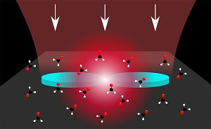
Researchers at the Harvard John A. Paulson School of Engineering and Applied Sciences (SEAS) have developed a new technique to squeeze infrared light into ultra-confined spaces, generating an intense, nanoscale antenna that could be used to detect single biomolecules.
The researchers harnessed the power of polaritons, particles that blur the distinction between light and matter. This ultra-confined light can be used to detect very small amounts of matter close to the polaritons. For example, many hazardous substances, such as formaldehyde, have an infrared signature that can be magnified by these antennas. The shape and size of the polaritons can also be tuned, paving the way to smart infrared detectors and biosensors.
“This work opens up a new frontier in nanophotonics,” said Federico Capasso, the Robert L. Wallace Professor of Applied Physics and Vinton Hayes Senior Research Fellow in Electrical Engineering, and senior author of the study. “By coupling light to atomic vibrations, we have concentrated light into nanodevices much smaller than its wavelength, giving us a new tool to detect and manipulate molecules.”
Polaritons are hybrid quantum mechanical particles, made up of a photon strongly coupled to vibrating atoms in a two-dimensional crystal.
“Our goal was to harness this strong interaction between light and matter and engineer polaritons to focus light in very small spaces,” said Michele Tamagnone, postdoctoral fellow in Applied Physics at SEAS and co-first author of the paper.
The researchers built nano-discs — the smallest about 50 nanometers high and 200 nanometers wide — made of two-dimensional boron nitride crystals. These materials act as micro-resonators, trapping infrared photons and generating polaritons. When illuminated with infrared light, the discs were able to concentrate light in a volume thousands of times smaller than is possible with standard optical materials, such as glass.
At such high concentrations, the researchers noticed something curious about the behavior of the polaritons: they oscillated like water sloshing in a glass, changing their oscillation depending on the frequency of the incident light.
These hybrid quantum mechanical particles oscillate like water sloshing in a glass, changing their oscillation depending on the frequency of the incident light. (Image courtesy of the Capasso Lab/Harvard SEAS)
“If you tip a cup back-and-forth, the water in the glass oscillates in one direction. If you swirl your cup, the water inside the glass oscillates in another direction. The polaritons oscillate in a similar way, as if the nano-discs are to light what a cup is to water,” said Tamagnone.
Unlike traditional optical materials, these boron nitride crystals are not limited in size by the wavelength of light, meaning there is no limit to how small the cup can be. These materials also have tiny optical losses, meaning that light confined to the disc can oscillate for a long time before it settles, making the light inside even more intense.
The researchers further concentrated light by placing two discs with matching oscillations next to each other, trapping light in the 50-nanometer gap between them and creating an infrared antenna. As light concentrates in smaller and smaller volumes, its intensity increases, creating optical fields so strong they can exert measurable force on nearby particles.
“These light-induced forces serve also as one our detection mechanisms,” said Antonio Ambrosio, a principal scientist at Harvard’s Center for Nanoscale Systems. “We observed this ultra-confined light by the motion it induces on an atomically sharp tip connected to a cantilever.”
A future challenge for the Harvard team is to optimize these light nano-concentrators to achieve intensities high enough to enhance the interaction with a single molecule to detectable values.
This research was co-authored by Kundan Chaudhary, Luis A. Jauregui, Philip Kim and William L. Wilson. It was supported by the National Science Foundation and the Swiss National Science Foundation.
Share on:


Testimonial
"We’re proud to call I-Connect007 a trusted partner. Their innovative approach and industry insight made our podcast collaboration a success by connecting us with the right audience and delivering real results."
Julia McCaffrey - NCAB GroupSuggested Items
I-Connect007 Launches Advanced Electronics Packaging Digest
09/15/2025 | I-Connect007I-Connect007 is pleased to announce the launch of Advanced Electronics Packaging Digest (AEPD), a new monthly digital newsletter dedicated to one of the most critical and rapidly evolving areas of electronics manufacturing: advanced packaging at the interconnect level.
Panasonic Industry will Double the Production Capacity of MEGTRON Multi-layer Circuit Board Materials Over the Next Five Years
09/15/2025 | Panasonic Industry Co., Ltd.Panasonic Industry Co., Ltd., a Panasonic Group company, announced plans for a major expansion of its global production capacity for MEGTRON multi-layer circuit board materials today. The company plans to double its production over the next five years to meet growing demand in the AI server and ICT infrastructure markets.
Trouble in Your Tank: Implementing Direct Metallization in Advanced Substrate Packaging
09/15/2025 | Michael Carano -- Column: Trouble in Your TankDirect metallization systems based on conductive graphite are gaining popularity throughout the world. The environmental and productivity gains achievable with this process are outstanding. Direct metallization reduces the costs of compliance, waste treatment, and legal issues related to chemical exposure. A graphite-based direct plate system has been devised to address these needs.
Fresh PCB Concepts: Designing for Success at the Rigid-flex Transition Area
08/28/2025 | Team NCAB -- Column: Fresh PCB ConceptsRigid-flex PCBs come in all shapes and sizes. Manufacturers typically use fire-retardant, grade 4 (FR-4) materials in the rigid section and flexible polyimide materials in the flex region. Because of the small size, some rigid-flex PCBs, like those for hearing aid devices, are among the most challenging to manufacture. However, regardless of its size, we should not neglect the transition area between the rigid and flexible material.
Global Sourcing Spotlight: How to Evaluate Supplier Capabilities Worldwide
08/20/2025 | Bob Duke -- Column: Global Sourcing SpotlightIn global sourcing, the difference between a competitive edge and a catastrophic disruption often comes down to how well you vet your suppliers. Sourcing advanced PCBs, precision components, or materials for complex assemblies demands diligence, skepticism, and more than a little time on airplanes. Here’s how to do your due diligence when evaluating international suppliers and why cutting corners can cost you more than money.