


 Trouble in Your Tank: Implementing Direct Metallization in Advanced Substrate Packaging
 It’s Only Common Sense: Storytelling That Sells—Stop Pitching, Start Painting Pictures
 The Right Approach: Get Ready for ISO 9001 Version 6


Researchers Solve Major Challenge in Mass Production of Low-Cost Solar Cells
June 22, 2018 | New York University Tandon School of EngineeringEstimated reading time: 4 minutes
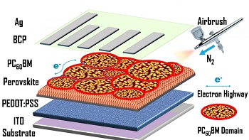
An international team of university researchers today reports solving a major fabrication challenge for perovskite cells — the intriguing potential challengers to silicon-based solar cells.
These crystalline structures show great promise because they can absorb almost all wavelengths of light. Perovskite solar cells are already commercialized on a small scale, but recent vast improvements in their power conversion efficiency (PCE) are driving interest in using them as low-cost alternatives for solar panels.
In the cover article published online today for the June 28, 2018 issue of Nanoscale, a publication of the Royal Society of Chemistry, the research team reveals a new scalable means of applying a critical component to perovskite cells to solve some major fabrication challenges. The researchers were able to apply the critical electron transport layer (ETL) in perovskite photovoltaic cells in a new way — spray coating — to imbue the ETL with superior conductivity and a strong interface with its neighbor, the perovskite layer.
The research is led by André D. Taylor, an associate professor in the NYU Tandon School of Engineering’s Chemical and Biomolecular Engineering Department, with Yifan Zheng, the first author on the paper and a Peking University researcher. Co-authors are from the University of Electronic Science and Technology of China, Yale University, and Johns Hopkins University.
Most solar cells are “sandwiches” of materials layered in such a way that when light hits the cell’s surface, it excites electrons in negatively charged material and sets up an electric current by moving the electrons toward a latticework of positively charged “holes.” In perovskite solar cells with a simple planar orientation called p-i-n (or n-i-p when inverted), the perovskite constitutes the light-trapping intrinsic layer (the “i” in p-i-n) between the negatively charged ETL and a positively charged hole transport layer (HTL).
When the positively and negatively charged layers are separated, the architecture behaves like a subatomic game of Pachinko in which photons from a light source dislodge unstable electrons from the ETL, causing them to fall toward the positive HTL side of the sandwich. The perovskite layer expedites this flow. While perovskite makes for an ideal intrinsic layer because of its strong affinity both for holes and electrons and its quick reaction time, commercial-scale fabrication has proved challenging partly because it is difficult to effectively apply a uniform ETL layer over the crystalline surface of the perovskite.
The researchers chose the compound [6,6]-phenyl-C(61)-butyric acid methyl ester (PCBM) because of its track record as an ETL material and because PCBM applied in a rough layer offers the possibility of improved conductivity, less-penetrable interface contact, and enhanced light trapping.
“Very little research has been done on ETL options for the planar p-i-n design,” said Taylor. “The key challenge in planar cells is, how do you actually assemble them in a way that doesn’t destroy the adjacent layers?”
The most common method is spin casting, which involves spinning the cell and allowing centripetal force to disperse the ETL fluid over the perovskite substrate. But this technique is limited to small surfaces and results in an inconsistent layer that lowers the performance of the solar cell. Spin casting is also inimicable to commercial production of large solar panels by such methods as roll-to-roll manufacture, for which the flexible p-i-n planar perovskite architecture is otherwise well suited.
The researchers instead turned to spray coating, which applies the ETL uniformly across a large area and is suitable for manufacturing large solar panels. They reported a 30 percent efficiency gain over other ETLs – from a PCE of 13 percent to over 17 percent – and fewer defects.
Added Taylor, “Our approach is concise, highly reproducible, and scalable. It suggests that spray coating the PCBM ETL could have broad appeal toward improving the efficiency baseline of perovskite solar cells and providing an ideal platform for record-breaking p-i-n perovskite solar cells in the near future.”
The Foundation of the National Natural Science Foundation of China (NSFC), the Foundation for Innovation Research Groups of the NSFC, the Chinese Scholarship Council, and the U.S. National Science Foundation provided funding for the study.
About the New York University Tandon School of Engineering
The NYU Tandon School of Engineering dates to 1854, the founding date for both the New York University School of Civil Engineering and Architecture and the Brooklyn Collegiate and Polytechnic Institute (widely known as Brooklyn Poly). A January 2014 merger created a comprehensive school of education and research in engineering and applied sciences, rooted in a tradition of invention and entrepreneurship and dedicated to furthering technology in service to society. In addition to its main location in Brooklyn, NYU Tandon collaborates with other schools within NYU, one of the country’s foremost private research universities, and is closely connected to engineering programs at NYU Abu Dhabi and NYU Shanghai. It operates Future Labs focused on start-up businesses in downtown Manhattan and Brooklyn and an award-winning online graduate program. For more information, visit engineering.nyu.edu.
Share on:


Testimonial
"In a year when every marketing dollar mattered, I chose to keep I-Connect007 in our 2025 plan. Their commitment to high-quality, insightful content aligns with Koh Young’s values and helps readers navigate a changing industry. "
Brent Fischthal - Koh YoungSuggested Items
ASM Technologies Limited signs MoU with the Guidance, Government of Tamilnadu to Expand Design-Led Manufacturing capabilities for ESDM
09/15/2025 | ASM TechnologiesASM Technologies Limited, a pioneer in Design- Led Manufacturing in the semiconductor and automotive industries, announced signing of Memorandum of Understanding (MoU) with the Guidance, Government of Tamilnadu whereby it will invest Rs. 250 crores in the state to expand its ESDM related Design-Led Manufacturing and precision engineering capacity. ASM Technologies will acquire 5 acres of land from the Government of Tamilnadu to set up a state-of-the-art design facility in Tamil Nadu's growing technology manufacturing ecosystem, providing a strong strategic advantage and long-term benefits for ASM.
Intel Announces Key Leadership Appointments to Accelerate Innovation and Strengthen Execution
09/09/2025 | Intel CorporationIntel Corporation today announced a series of senior leadership appointments that support the company’s strategy to strengthen its core product business, build a trusted foundry, and foster a culture of engineering across the business.
Cadence to Acquire Hexagon’s Design & Engineering Business
09/08/2025 | Cadence Design SystemsCadence announced it has entered into a definitive agreement to acquire the Design & Engineering (D&E) business of Hexagon AB, which includes its MSC Software business—a pioneer in engineering simulation and analysis solutions.
Marcy’s Musings: Continuing to Invent the Future With SEL
08/19/2025 | Marcy LaRont -- Column: Marcy's MusingsTwo years ago, PCB007 Magazine devoted an issue to Schweitzer Engineering Labs (SEL), a new captive greenfield PCB facility in Moscow, Idaho. We highlighted some of the most cutting-edge achievements in facility layout, design, and equipment in the PCB fabrication industry. SEL was a shining example of what was possible, providing insight and inspiration to PCB fabricators looking toward growth and expansion.
Advint and SanRex Expand High-Performance DC Rectifier Access for North American PCB Fabricators
08/12/2025 | Advint IncorporatedAdvint Incorporated has entered a strategic partnership with SanRex Corporation, enhancing access to industrial-grade DC rectifiers for the US printed circuit board industry. With a legacy of power innovation and performance across the globe, SanRex rectifiers are available through Advint’s proficient distribution network.