


 Dan’s Biz Bookshelf: ‘The Next RenAIssance: AI and the Expansion of Human Potential’
 The Chemical Connection: When the Industry Moves Faster Than the Standards
 Driving Innovation: Selecting the Right Laser Source


3Q18 Contract Price Hike for Server DRAM Limited Due to Improved Supply
June 25, 2018 | TrendForceEstimated reading time: 1 minute
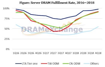
The shortfall in the supply of server DRAM may ease in the second half, as evidenced by the increasing average shipment fulfillment rate in the past several quarters, according to DRAMeXchange, a division of TrendForce.
As a result, following the 10% sequential hike in contract prices in the first half, the average shipment fulfillment rate has topped 80% now, thanks to the adjustment of output share of server DRAM by DRAM suppliers, which has helped to ease the tight supply situation, says Mark Liu, the senior analyst of DRAMeXchange.
DRAMeXchange points out that the prices of 32 GB server modules to be shipped to the first-tier firms in Q3 may advance by 1-2% to US$320. Meanwhile, second-tier makers will become benefited thanks to increased shipment fulfillment rates. Consequently, the range of quotes for Q3 contract prices will be limited.
Meanwhile, affected by the increased penetration rates of Intel’s Purley and AMD’s Naples platform, the average density and penetration rate of 32 GB product lines will increase in the second half, sustaining the demands for server DRAM. The stocking-up demands for Intel's new solutions will remain robust, with shipment still mainly for data centers in North America and China. The penetration rate of Intel’s Purley platform is expected to approach 80% in Q4, up from over 50% now, while penetration rate of 32 GB server modules will exceed 70% by the end of the year, according to DRAMeXchange.
In terms of the development of process technology, 20 nm will remain the mainstream process for DRAM this year and stocking-up demands for high-density server modules will continue to the end of the year, thanks to the effect of new platform solutions. Currently, the share of products featuring advanced process remaining low. In addition, die shrink technology will become increasingly complicated after the migration to 17 nm and 18 nm processes. Therefore, except Samsung which has applied 18 nm process in the mass production of server products, other DRAM suppliers will not begin increasing the share of products with advanced process until Q4, due to the consideration of product reliability.
Share on:


Subscribe
Stay ahead of the technologies shaping the future of electronics with our latest newsletter, Advanced Electronics Packaging Digest. Get expert insights on advanced packaging, materials, and system-level innovation, delivered straight to your inbox.Subscribe now to stay informed, competitive, and connected.
Suggested Items
The Missing Connection: Wire Harness Quoting Joins the Digital Age
05/01/2026 | Joanne Harris, Tech-2marketingWalk the floor of a modern wire harness manufacturing facility, and the investment in technology is hard to miss. Automated wire cutting and stripping machines process thousands of cuts an hour with sub-millimeter precision. Computerized crimping presses deliver consistent, validated terminations that a hand tool never could. Laser wire markers, automated test benches, and vision-guided assembly stations represent hundreds of thousands of dollars of capital investment, all in service of building a better harness faster and more reliably than the competition.
EDADOC: Building the ‘Neural Hub’ for High-Compute Chips Within a Compact Space
04/28/2026 | ECIOEvery chip to the market must pass a stringent checkpoint before shipment known as ATE testing. Serving as the physical “neural hub” that connects test equipment worth millions of dollars with the device under test, the performance of the ATE test board directly determines the accuracy, efficiency, and final yield of chip testing. Amid the rapid rise of high-compute chips, what extreme challenges is this seemingly small circuit board facing? How is EDADOC addressing industry pain points through its one-stop “design + manufacturing” model?
The Chemical Connection: When the Industry Moves Faster Than the Standards
04/29/2026 | Don Ball -- Column: The Chemical ConnectionAs a supplier of wet processing equipment, we have rules and standards we must adhere to, including both regional and national electrical codes and safety and environmental regulations, as well as myriad other standards to make the equipment safe to use. Things are a little different when it comes to rules and standards for manufacturing PCBs, though, because technical advances and requirements change so quickly that standards can’t keep up.
Driving Innovation: Selecting the Right Laser Source
04/28/2026 | Simon Khesin -- Column: Driving InnovationWhen I first joined Schmoll Maschinen, I brought experience from almost every PCB process, except for laser. As I immersed myself in laser processing, I realized why it can seem so daunting to a newcomer. The complexity arises from three intersecting factors: A vast variety of laser sources: CO2, UV-nano, green-pico, UV-pico, IR-pico, and others; a diverse range of applications: Drilling, cutting, ablation, and more; and an extensive list of materials: These have vastly different absorption rates. Choosing the right machine or laser source is rarely trivial. Even for experienced engineers, answering "Which source is best?" requires examining the business's specific goals.
Market Insights with Pluritec's Maurizio Bonati
04/23/2026 | Real Time with... APEX EXPONolan Johnson interviews Maurizio Bonati, VP of Sales at Pluritec, at APEX EXPO 2026. Bonati details Pluritec's three product divisions, covering a broad spectrum of PCB manufacturing. He discusses the current robust electronics market, driven by AI applications in Asia and technological investments in North America, while noting slower demand in Europe. The interview highlights key sectors like data centers, AI, and medical that benefit from advanced electronics.