


 Driving Innovation: Mechanical and Optical Processes During Rigid-flex Production
 It’s Only Common Sense: Your Biggest Competitor Is Complacency
 The Chemical Connection: Onshoring PCB Production—Daunting but Certainly Possible


Biosensor Chip Detects Single Nucleotide Polymorphism Wirelessly and With Higher Sensitivity
July 10, 2018 | University of California San DiegoEstimated reading time: 3 minutes
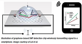
A team led by the University of California San Diego has developed a chip that can detect a type of genetic mutation known as a single nucleotide polymorphism (SNP) and wirelessly send the results in real time to a smartphone, computer, or other electronic device. The chip is at least 1,000 times more sensitive at detecting an SNP than current technology.
The advance, published July 9 in Advanced Materials, could lead to cheaper, faster and portable biosensors for early detection of genetic markers for diseases such as cancer.
An SNP is the change in a single nucleotide base (A, C, G or T) in the DNA sequence. It is the most common type of genetic mutation. While most SNPs have no discernible effect on health, some are associated with increased risk of developing pathological conditions such as cancer, diabetes, heart disease, neurodegenerative disorders, autoimmune and inflammatory diseases.
Traditional SNP detection methods have several limitations: they have relatively poor sensitivity and specificity; they require amplification to get multiple copies for detection; they require the use of bulky instruments; and they cannot work wirelessly.
The new DNA biosensor developed by the UC San Diego-led team is a wireless chip that’s smaller than a fingernail and can detect an SNP that’s present in picomolar concentrations in solution.
“Miniaturized chip-based electrical detection of DNA could enable in-field and on-demand detection of specific DNA sequences and polymorphisms for timely diagnosis or prognosis of pending health crises, including viral and bacterial infection-based epidemics,” said Ratnesh Lal, professor of bioengineering, mechanical engineering and materials science at the UC San Diego Jacobs School of Engineering.
The chip essentially captures a strand of DNA containing a specific SNP mutation and then produces an electrical signal that is sent wirelessly to a mobile device. It consists of a graphene field effect transistor with a specially engineered piece of double stranded DNA attached to the surface. This piece of DNA is bent near the middle and shaped like a pair of tweezers. One side of these so-called “DNA-tweezers” codes for a specific SNP. Whenever a DNA strand with that SNP approaches, it binds to that side of the DNA-tweezers, opening them up and creating a change in electrical current that is detected by the graphene field effect transistor.
The project is led by Lal and involves teams at the Institute of Engineering in Medicine at UC San Diego, Chinese Academy of Sciences in China, University of Pennsylvania, Max Planck Institute for Biophysical Chemistry in Germany, and Inner Mongolia Agricultural University in China.
DNA Strand Displacement
What drives this technology is a molecular process called DNA strand displacement—when a DNA double helix exchanges one of its strands for a new complementary strand. In this case, the DNA-tweezers swap one their strands for one with a particular SNP.
This is possible due to the particular way the DNA-tweezers are engineered. One of the strands is a “normal” strand that is attached to the graphene transistor and contains the complementary sequence for a specific SNP. The other is a “weak” strand in which some of the nucleotides are replaced with a different molecule to weaken its bonds to the normal strand. A strand containing the SNP is able to bind more strongly to the normal strand and displace the weak strand. This leaves the DNA-tweezers with a net electric charge that can be easily detected by the graphene transistor.
This work builds upon the first label- and amplification-free electronic SNP detection chip that Lal’s team previously developed in collaboration with Gennadi Glinksy, a research scientist at the UC San Diego Institute of Engineering in Medicine, and other UC San Diego researchers. The new chip has added wireless capability and is at least 1,000 times more sensitive than its predecessor.
What makes the new chip so sensitive is the design of the DNA-tweezers. When the SNP-containing strand binds, it opens up the DNA-tweezers, changing their geometry so that they become almost parallel to the graphene surface. This brings the net electric charge of the DNA close to the graphene surface, giving a larger signal. In contrast, the DNA probe built into the previous chip has a structure that cannot be brought closer to the graphene surface, so it generates a weaker signal upon binding an SNP-containing strand.
Next steps include designing array chips to detect up to hundreds of thousands of SNPs in a single test. Future studies will involve testing the chip on blood and other bodily fluid samples taken from animals or humans.
Share on:


Testimonial
"Our marketing partnership with I-Connect007 is already delivering. Just a day after our press release went live, we received a direct inquiry about our updated products!"
Rachael Temple - AlltematedSuggested Items
Beyond Thermal Conductivity: Exploring Polymer-based TIM Strategies for High-power-density Electronics
10/13/2025 | Padmanabha Shakthivelu and Nico Bruijnis, MacDermid Alpha Electronics SolutionsAs power density and thermal loads continue to increase, effective thermal management becomes increasingly important. Rapid and efficient heat transfer from power semiconductor chip packages is essential for achieving optimal performance and ensuring long-term reliability of temperature-sensitive components. This is particularly crucial in power systems that support advanced applications such as green energy generation, electric vehicles, aerospace, and defense, along with high-speed computing for data centers and artificial intelligence (AI).
Driving Innovation: Depth Routing Processes—Achieving Unparalleled Precision in Complex PCBs
09/08/2025 | Kurt Palmer -- Column: Driving InnovationIn PCB manufacturing, the demand for increasingly complex and miniaturized designs continually pushes the boundaries of traditional fabrication methods, including depth routing. Success in these applications demands not only on robust machinery but also sophisticated control functions. PCB manufacturers rely on advanced machine features and process methodologies to meet their precise depth routing goals. Here, I’ll explore some crucial functions that empower manufacturers to master complex depth routing challenges.
Polar Instruments Announces Additive Transmission Line Support for Si9000e
08/20/2025 | Polar InstrumentsTransmission lines embedded into the PCB surface are a feature of UHDI constructions. The 2025 fall release of Polar's Si9000e PCB impedance & insertion loss transmission line field solver incorporates eight new single ended, differential and coplanar transmission line structures.
Henniker Plasma Launches Stratus Turnkey Plasma Manufacturing Cell
08/13/2025 | Henniker PlasmaHenniker Plasma, a leading manufacturer of plasma treatment systems, proudly announces the launch of its Stratus Plasma Manufacturing Cell range — a fully integrated, turnkey solution that combines advanced atmospheric plasma surface treatment with robotic automation.
Trouble in Your Tank: Metallizing Flexible Circuit Materials—Mitigating Deposit Stress
08/04/2025 | Michael Carano -- Column: Trouble in Your TankMetallizing materials, such as polyimide used for flexible circuitry and high-reliability multilayer printed wiring boards, provide a significant challenge for process engineers. Conventional electroless copper systems often require pre-treatments with hazardous chemicals or have a small process window to achieve uniform coverage without blistering. It all boils down to enhancing the adhesion of the thin film of electroless copper to these smooth surfaces.