


 The Chemical Connection Onshoring PCB Production—Daunting but Certainly Possible
 It’s Only Common Sense: The Phone Is Still Mightier Than the Keyboard


Nanocrystal Links Could Lead to Better Electronics
July 17, 2018 | University of ChicagoEstimated reading time: 2 minutes
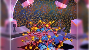
Chemists and engineers today are very interested in a kind of nanotechnology enabled by tiny islands of nanoparticles called “colloidal nanocrystals.” They can be made out of abundant and non-toxic materials, and they can be easily tweaked to have a number of different properties as a function of their size. Depending on how they’re built, colloidal nanocrystals could be made into solar panels, electronics or optical devices. But all of these applications require making nanocrystals friendly places for electrons to travel along.
A new study published in Nature Nanotechnology helps fill in the cracks for scientists trying to use nanocrystals to design better electronic and optoelectronic devices. According to research by University of Chicago, Argonne National Laboratory and Max Planck Institute for Iron Research scientists, inorganic links between the nanoparticles themselves are changing and reforming on the surface of the nanoparticles.
The team focused on the links between nanoparticles. At first, scientists used organic molecules to link them, but these tended to block the movement of electrons. Some recent experiments have seen much better results for inorganic molecules instead, but no one was sure why. “We never had an atomistic model for the behavior of these inorganic linkers,” said study co-author Giulia Galli, the Liew Family Professor of Molecular Engineering and professor of chemistry at the University of Chicago and a senior scientist at Argonne.
Galli worked with colleague Dmitri Talapin, the Louis Block Distinguished Service Professor of Chemistry and a scientist at Argonne, as well as Stefan Wippermann, group leader at the Max Planck Institute, to explore the structure of nanocrystals made with these inorganic links.
Through a combination of theory and experiment, the team puzzled out the blow-by-blow of actions. It turns out that the linker molecules react where they’re attached and form a sort of glue, which affects the properties of the nanoparticles. “Instead of each having separate identities, the whole thing should really be considered as a complex nanomaterial,” Galli said. “This was totally different from what was thought.”
“The complete model of the structural properties of the nanoparticles should help scientists and engineers as they try to design materials for better and less toxic electronics, solar panels and more,” said Wippermann, who led the study.
“The computational machinery developed during this study is rather unique and should be applicable to a broad range of nanostructured materials containing both crystalline and amorphous components,” said Talapin.
Both Wipperman and first author Emilio Scalise are from the Max Planck Institute for Iron Research. Other UChicago authors were graduate students Vishwas Srivastava and Eric Janke.
By Louise Lerner
Share on:


Testimonial
"Advertising in PCB007 Magazine has been a great way to showcase our bare board testers to the right audience. The I-Connect007 team makes the process smooth and professional. We’re proud to be featured in such a trusted publication."
Klaus Koziol - atgSuggested Items
ITW EAE Despatch Ovens Now Support ASTM 5423 Testing
10/15/2025 | ITW EAEAs the demand for high-performance electrical insulation materials continues to grow—driven by the rapid expansion of electric vehicles (EVs) and energy storage systems—thermal processing has become a critical step in material development.
Beyond Thermal Conductivity: Exploring Polymer-based TIM Strategies for High-power-density Electronics
10/13/2025 | Padmanabha Shakthivelu and Nico Bruijnis, MacDermid Alpha Electronics SolutionsAs power density and thermal loads continue to increase, effective thermal management becomes increasingly important. Rapid and efficient heat transfer from power semiconductor chip packages is essential for achieving optimal performance and ensuring long-term reliability of temperature-sensitive components. This is particularly crucial in power systems that support advanced applications such as green energy generation, electric vehicles, aerospace, and defense, along with high-speed computing for data centers and artificial intelligence (AI).
Is Glass Finally Coming of Age?
10/13/2025 | Nolan Johnson, I-Connect007Substrates, by definition, form the base of all electronic devices. Whether discussing silicon wafers for semiconductors, glass-and-epoxy materials in printed circuits, or the base of choice for interposers, all these materials function as substrates. While other substrates have come and gone, silicon and FR-4 have remained the de facto standards for the industry.
Creative Materials to Showcase Innovative Functional Inks for Medical Devices at COMPAMED 2025
10/09/2025 | Creative Materials, Inc.Creative Materials, a leading manufacturer of high-performance functional inks and coatings, is pleased to announce its participation in COMPAMED 2025, taking place November 17–20 in Düsseldorf, Germany.
Jiva Leading the Charge Toward Sustainable Innovation
09/30/2025 | Marcy LaRont, PCB007 MagazineEnvironmental sustainability in business—product circularity—is a high priority these days. “Circularity,” the term meant to replace “recycling,” in its simplest definition, describes a full circle life for electronic products and all their elements. The result is re-use or a near-complete reintroduction of the base materials back into the supply chain, leaving very little left for waste. For what cannot be reused productively, the ultimate hope is to have better, less harmful means of disposal and/or materials that can seamlessly and harmlessly decompose and integrate back into the natural environment. That is where Jiva and Soluboard come in.