


 It’s Only Common Sense: Hire for Hunger, Train for Skill
 Dan’s Biz Bookshelf: ‘The 'NVIDIA Way: Jensen Huang and the Making of a Tech Giant’


Electronic Stickers to Streamline Large-Scale 'Internet of Things'
July 17, 2018 | Purdue UniversityEstimated reading time: 2 minutes
Billions of objects ranging from smartphones and watches to buildings, machine parts and medical devices have become wireless sensors of their environments, expanding a network called the "Internet of Things."
As society moves toward connecting all objects to the internet – even furniture and office supplies – the technology that enables these objects to communicate and sense each other will need to scale up.
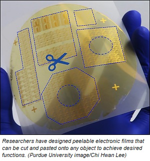
Researchers at Purdue University and the University of Virginia have developed a new fabrication method that makes tiny, thin-film electronic circuits peelable from a surface. The technique not only eliminates several manufacturing steps and the associated costs, but also allows any object to sense its environment or be controlled through the application of a high-tech sticker.
Eventually, these stickers could also facilitate wireless communication. The researchers demonstrate capabilities on various objects in a paper recently published in the Proceedings of the National Academy of Sciences.
"We could customize a sensor, stick it onto a drone, and send the drone to dangerous areas to detect gas leaks, for example," said Chi Hwan Lee, Purdue assistant professor of biomedical engineering and mechanical engineering.
*Most of today’s electronic circuits are individually built on their own silicon “wafer,” a flat and rigid substrate. The silicon wafer can then withstand the high temperatures and chemical etching that are used to remove the circuits from the wafer.
But high temperatures and etching damage the silicon wafer, forcing the manufacturing process to accommodate an entirely new wafer each time.
Lee’s new fabrication technique, called “transfer printing,” cuts down manufacturing costs by using a single wafer to build a nearly infinite number of thin films holding electronic circuits. Instead of high temperatures and chemicals, the film can peel off at room temperature with the energy-saving help of simply water.
“It’s like the red paint on San Francisco’s Golden Gate Bridge – paint peels because the environment is very wet,” Lee said. “So in our case, submerging the wafer and completed circuit in water significantly reduces the mechanical peeling stress and is environmentally friendly.”
A ductile metal layer, such as nickel, inserted between the electronic film and the silicon wafer, makes the peeling possible in water. These thin-film electronics can then be trimmed and pasted onto any surface, granting that object electronic features.
Putting one of the stickers on a flower pot, for example, made that flower pot capable of sensing temperature changes that could affect the plant’s growth.
Lee’s lab also demonstrated that the components of electronic integrated circuits work just as well before and after they were made into a thin film peeled from a silicon wafer. The researchers used one film to turn on and off an LED light display.
“We’ve optimized this process so that we can delaminate electronic films from wafers in a defect-free manner,” Lee said.
A YouTube video is available below:
Share on:


Testimonial
"In a year when every marketing dollar mattered, I chose to keep I-Connect007 in our 2025 plan. Their commitment to high-quality, insightful content aligns with Koh Young’s values and helps readers navigate a changing industry. "
Brent Fischthal - Koh YoungSuggested Items
MEIKO Electronics Expands ASEAN Footprint with New Vietnam Subsidiary to Support Growing Demand
04/16/2026 | MeikoMEIKO ELECTRONICS CO., LTD. has announced that, at its Board of Directors meeting held on April 8, 2026, the company resolved to establish a wholly owned subsidiary, MEIKO ELECTRONICS YEN QUANG CO., LTD. (MKYQ), in Phu Tho Province, Vietnam.
Alpha and Omega Semiconductor Begins IPM5 Production at Kaynes Semicon Launch in Gujarat
04/16/2026 | Alpha and Omega Semiconductor LimitedAlpha and Omega Semiconductor Limited, a designer, developer, and global supplier of a broad range of discrete power devices, wide bandgap power devices, power management ICs, and modules, marks a historic expansion of its global manufacturing footprint with the official inauguration of Kaynes Semicon’s state-of-the-art OSAT facility in Sanand, Gujarat.
Podcast Hits the Mark in a Materials Market
04/15/2026 | Marcy LaRont, I-Connect007The base material of a printed circuit board is its literal and functional foundation. Isola, founded in 1912 in Düren, Germany, is one of the longest-standing manufacturers of glass-reinforced laminates in the electronics industry. Originally focused on insulation and fiberglass materials, the company played an early role in supplying the foundational substrates that enabled the growth of PCB technology. As electronics advanced, Isola evolved alongside the industry, expanding from basic glass-epoxy laminates into high-performance copper-clad materials and engineered prepregs.
Inside Eastek Malaysia: Scalable Manufacturing Built on Trust, Stability, and Technical Expertise
04/14/2026 | Eastek International CorporationEastek International Corporation continues to strengthen its global manufacturing platform through the sustained performance and expanding capabilities of its Malaysia operation.
SMTA Ultra HDI Symposium, Day 1: AI at the Core or Out of the Game
04/13/2026 | Marcy LaRont, I-Connect007It was a beautiful 81°F morning in Arizona last Wednesday as I headed to the third annual SMTA Ultra HDI Symposium, focused on AI and ultra high density interconnect technology. Strategically held as part of Arizona’s Tech Week, this year’s conference took place in Avondale in Phoenix's West Valley. The event moved from the cozy offices of the Peoria Sports Complex (which paid homage to baseball’s spring training world) to the larger Avondale Conference Center, highlighting the importance of this area for electronics manufacturing investment.