


 Trouble in Your Tank: Implementing Direct Metallization in Advanced Substrate Packaging
 It’s Only Common Sense: Storytelling That Sells—Stop Pitching, Start Painting Pictures
 The Right Approach: Get Ready for ISO 9001 Version 6


Using Spin Current to Convert Mechanical Vibrations Into Electricity
July 20, 2018 | RIKENEstimated reading time: 2 minutes
A nanoscale device that converts mechanical ripples into an electrical current via a ‘spin current’ has been made by RIKEN researchers1. Further development of this technology could see it used in devices that permit sound waves to pass in one direction but block them in the opposite direction.
Conventional electronic devices are based on shunting electrons around circuits. Because electrons possess charge, they give rise to electric currents when they move. The emerging field of spintronics, however, harnesses another property of electrons: their spin. Spin currents are the spintronic equivalent of electric currents, but unlike electric currents, they can flow without the electrons actually moving since spin can be transferred between stationary electrons.
As well as holding out the promise of resistance-free energy flow, electron spin can be used to convert between various forms of energy, including electricity, light, sound, vibrations and heat. This ability to switch between different energy forms will lead to a wide range of versatile devices.
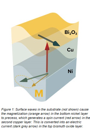
Jorge Puebla at the RIKEN Center for Emergent Matter Science and Mingran Xu at the University of Tokyo and colleagues have made a three-layered nanodevice that converts mechanical vibrations into electric current. Waves generated on the surface of a substrate cause the magnetization of the bottom nickel layer of the device to sweep out arcs (Fig. 1). This periodic motion of the magnetization generates a spin current in the second copper layer. Finally, the spin current is converted into an electric current at the interface with the top bismuth oxide layer.
The team found that the spin current generated in the second layer was particularly large. “In our field, researchers are seeking to generate higher spin currents,” explains Xu. “Our method produces quite a huge spin current.”
“We’re approaching spin currents that are large enough to move magnetic domain walls, which could be used in memory devices,” adds Puebla. “We’re still below the spin currents needed, but believe we should be able to get close by optimizing our devices.”
Another advance was the use of a relatively new way to convert a spin current into an electrical one. Often expensive metals such as platinum are required for this conversion, but the method the team used worked with copper. “I think in terms of technology, people might find this approach cheaper to produce real devices,” comments Xu.
Since the output varied with direction, a potential application is audio devices that allow sound to flow in one direction but not the opposite one. “You could have headphones that allow you to listen to music and hear what others are saying, but other people cannot hear what you’re listening to,” says Puebla.
Share on:


Testimonial
"Advertising in PCB007 Magazine has been a great way to showcase our bare board testers to the right audience. The I-Connect007 team makes the process smooth and professional. We’re proud to be featured in such a trusted publication."
Klaus Koziol - atgSuggested Items
Trouble in Your Tank: Implementing Direct Metallization in Advanced Substrate Packaging
09/15/2025 | Michael Carano -- Column: Trouble in Your TankDirect metallization systems based on conductive graphite are gaining popularity throughout the world. The environmental and productivity gains achievable with this process are outstanding. Direct metallization reduces the costs of compliance, waste treatment, and legal issues related to chemical exposure. A graphite-based direct plate system has been devised to address these needs.
Closing the Loop on PCB Etching Waste
09/09/2025 | Shawn Stone, IECAs the PCB industry continues its push toward greener, more cost-efficient operations, Sigma Engineering’s Mecer System offers a comprehensive solution to two of the industry’s most persistent pain points: etchant consumption and rinse water waste. Designed as a modular, fully automated platform, the Mecer System regenerates spent copper etchants—both alkaline and acidic—and simultaneously recycles rinse water, transforming a traditionally linear chemical process into a closed-loop system.
Driving Innovation: Depth Routing Processes—Achieving Unparalleled Precision in Complex PCBs
09/08/2025 | Kurt Palmer -- Column: Driving InnovationIn PCB manufacturing, the demand for increasingly complex and miniaturized designs continually pushes the boundaries of traditional fabrication methods, including depth routing. Success in these applications demands not only on robust machinery but also sophisticated control functions. PCB manufacturers rely on advanced machine features and process methodologies to meet their precise depth routing goals. Here, I’ll explore some crucial functions that empower manufacturers to master complex depth routing challenges.
Trouble in Your Tank: Minimizing Small-via Defects for High-reliability PCBs
08/27/2025 | Michael Carano -- Column: Trouble in Your TankTo quote the comedian Stephen Wright, “If at first you don’t succeed, then skydiving is not for you.” That can be the battle cry when you find that only small-diameter vias are exhibiting voids. Why are small holes more prone to voids than larger vias when processed through electroless copper? There are several reasons.
The Government Circuit: Navigating New Trade Headwinds and New Partnerships
08/25/2025 | Chris Mitchell -- Column: The Government CircuitAs global trade winds continue to howl, the electronics manufacturing industry finds itself at a critical juncture. After months of warnings, the U.S. Government has implemented a broad array of tariff increases, with fresh duties hitting copper-based products, semiconductors, and imports from many nations. On the positive side, tentative trade agreements with Europe, China, Japan, and other nations are providing at least some clarity and counterbalance.