


 Trouble in Your Tank: Implementing Direct Metallization in Advanced Substrate Packaging
 It’s Only Common Sense: Storytelling That Sells—Stop Pitching, Start Painting Pictures
 The Right Approach: Get Ready for ISO 9001 Version 6


Engineers Develop Efficient Semiconductor Material for Thermal Management
July 20, 2018 | UCLAEstimated reading time: 2 minutes
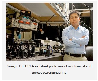
Working to address “hotspots” in computer chips that degrade their performance, UCLA engineers have developed a new semiconductor material, defect-free boron arsenide, that is more effective at drawing and dissipating waste heat than any other known semiconductor or metal materials.
This could potentially revolutionize thermal management designs for computer processors and other electronics, or for light-based devices like LEDs.
Computer processors have continued to shrink down to nanometer sizes where today there can be billions of transistors are on a single chip. This phenomenon is described under Moore’s Law, which predicts that the number of transistors on a chip will double about every two years. Each smaller generation of chips helps make computers faster, more powerful and able to do more work. But doing more work also means they’re generating more heat.
Managing heat in electronics has increasingly become one of the biggest challenges in optimizing performance. High heat is an issue for two reasons. First, as transistors shrink in size, more heat is generated within the same footprint. This high heat slows down processor speeds, in particular at “hotspots” on chips where heat concentrates and temperatures soar. Second, a lot of energy is used to keep those processors cool. If CPUs did not get as hot in the first place, then they could work faster and much less energy would be needed to keep them cool.
Image caption: Illustration showing a schematic of a computer chip with a hotspot (bottom); an electron microscope image of defect-free boron arsenide (middle); and an image showing electron diffraction patterns in boron arsenide. Image credit: Hu Research Lab/UCLA Samueli
The UCLA study was the culmination of several years of research by Hu and his students that included designing and making the materials, predictive modeling, and precision measurements of temperatures.
The defect-free boron arsenide, which was made for first time by the UCLA team, has a record-high thermal conductivity, more than three-times faster at conducting heat than currently used materials, such as silicon carbide and copper, so that heat that would otherwise concentrate in hotspots is quickly flushed away.
“This material could help greatly improve performance and reduce energy demand in all kinds of electronics, from small devices to the most advanced computer data center equipment,” Hu said. “It has excellent potential to be integrated into current manufacturing processes because of its semiconductor properties and the demonstrated capability to scale-up this technology. It could replace current state-of-the-art semiconductor materials for computers and revolutionize the electronics industry.”
In addition to the impact for electronic and photonics devices, the study also revealed new fundamental insights into the physics of how heat flows through a material.
“This success exemplifies the power of combining experiments and theory in new materials discovery, and I believe this approach will continue to push the scientific frontiers in many areas, including energy, electronics, and photonics applications,” Hu said.
The research was funded by the National Science Foundation, the Air Force Office of Scientific Research, the American Chemical Society’s Petroleum Research Fund, UCLA’s Sustainable LA Grand Challenge, and the Anthony and Jeanne Pritzker Family Foundation.
Share on:


Testimonial
"In a year when every marketing dollar mattered, I chose to keep I-Connect007 in our 2025 plan. Their commitment to high-quality, insightful content aligns with Koh Young’s values and helps readers navigate a changing industry. "
Brent Fischthal - Koh YoungSuggested Items
I-Connect007 Launches Advanced Electronics Packaging Digest
09/15/2025 | I-Connect007I-Connect007 is pleased to announce the launch of Advanced Electronics Packaging Digest (AEPD), a new monthly digital newsletter dedicated to one of the most critical and rapidly evolving areas of electronics manufacturing: advanced packaging at the interconnect level.
Global Interposer Market to Surge Nearly Fivefold by 2034
09/15/2025 | I-Connect007 Editorial TeamRevenue for the global interposer market is projected to climb from $471 million in 2025 to more than $2.3 billion by 2034, according to a new report from Business Research Insights. The growth represents a CAGR of nearly 20 percent over the forecast period.
ICAPE Group Unveils Exclusive Report on Sustainability in Electronics Manufacturing
09/15/2025 | ICAPE GroupICAPE Group, a global leader in printed circuit boards (PCBs) and custom electronics manufacturing, today announces the launch of its 2025 Industry Outlook & Innovation Report: Sustainability in Electronics Manufacturing. This exclusive report is accompanied by fresh insights from a dedicated Statista survey of 100 electronics manufacturing professionals, commissioned by ICAPE Group.
Sustainability and Selective Soldering
09/15/2025 | Dr. Samuel J. McMaster, Pillarhouse InternationalSustainability is more than just a buzzword for the electronics industry; it’s a key goal for all manufacturing processes. This is more than a box-ticking exercise or simply doing a small part for environmentally friendly processes. Moving toward sustainable solutions drives innovation and operational efficiency.
Smartphone Production Rises 4% QoQ in 2Q25 as Inventory Adjustment Ends
09/12/2025 | TrendForceTrendForce’s latest investigations reveal that global smartphone production reached 300 million units in 2Q25, up 4% QoQ and 4.8% YoY, driven by seasonal demand and the recovery of brands such as Oppo and Transsion following inventory adjustments.