


 The Chemical Connection: Onshoring PCB Production—Daunting but Certainly Possible
 It’s Only Common Sense: The Phone Is Still Mightier Than the Keyboard


NIST Chip Lights Up Optical Neural Network Demo
July 27, 2018 | NISTEstimated reading time: 2 minutes
Researchers at the National Institute of Standards and Technology (NIST) have made a silicon chip that distributes optical signals precisely across a miniature brain-like grid, showcasing a potential new design for neural networks.
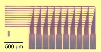
Image caption: NIST’s grid-on-a-chip distributes light signals precisely, showcasing a potential new design for neural networks. The three-dimensional structure enables complex routing schemes, which are necessary to mimic the brain. Light could travel farther and faster than electrical signals.
The human brain has billions of neurons (nerve cells), each with thousands of connections to other neurons. Many computing research projects aim to emulate the brain by creating circuits of artificial neural networks. But conventional electronics, including the electrical wiring of semiconductor circuits, often impedes the extremely complex routing required for useful neural networks.
The NIST team proposes to use light instead of electricity as a signaling medium. Neural networks already have demonstrated remarkable power in solving complex problems, including rapid pattern recognition and data analysis. The use of light would eliminate interference due to electrical charge, and the signals would travel faster and farther.
“Light’s advantages could improve the performance of neural nets for scientific data analysis such as searches for Earth-like planets and quantum information science, and accelerate the development of highly intuitive control systems for autonomous vehicles,” NIST physicist Jeff Chiles said.
A conventional computer processes information through algorithms, or human-coded rules. By contrast, a neural network relies on a network of connections among processing elements, or neurons, which can be trained to recognize certain patterns of stimuli. A neural or neuromorphic computer would consist of a large, complex system of neural networks.
Described in a new paper, the NIST chip overcomes a major challenge to the use of light signals by vertically stacking two layers of photonic waveguides—structures that confine light into narrow lines for routing optical signals, much as wires route electrical signals. This three-dimensional (3D) design enables complex routing schemes, which are necessary to mimic neural systems. Furthermore, this design can easily be extended to incorporate additional waveguiding layers when needed for more complex networks.
The stacked waveguides form a three-dimensional grid with 10 inputs or “upstream” neurons each connecting to 10 outputs or “downstream” neurons, for a total of 100 receivers. Fabricated on a silicon wafer, the waveguides are made of silicon nitride and are each 800 nanometers (nm) wide and 400 nm thick. Researchers created software to automatically generate signal routing, with adjustable levels of connectivity between the neurons.
Laser light was directed into the chip through an optical fiber. The goal was to route each input to every output group, following a selected distribution pattern for light intensity or power. Power levels represent the pattern and degree of connectivity in the circuit. The authors demonstrated two schemes for controlling output intensity: uniform (each output receives the same power) and a “bell curve” distribution (in which middle neurons receive the most power, while peripheral neurons receive less).
To evaluate the results, researchers made images of the output signals. All signals were focused through a microscope lens onto a semiconductor sensor and processed into image frames. This method allows many devices to be analyzed at the same time with high precision. The output was highly uniform, with low error rates, confirming precise power distribution.
“We’ve really done two things here,” Chiles said. “We’ve begun to use the third dimension to enable more optical connectivity, and we’ve developed a new measurement technique to rapidly characterize many devices in a photonic system. Both advances are crucial as we begin to scale up to massive optoelectronic neural systems.”
Share on:


Testimonial
"In a year when every marketing dollar mattered, I chose to keep I-Connect007 in our 2025 plan. Their commitment to high-quality, insightful content aligns with Koh Young’s values and helps readers navigate a changing industry. "
Brent Fischthal - Koh YoungSuggested Items
PDN Optimization: Balancing Performance and Cost in SoC Designs
10/22/2025 | Zach Caprai. Siemens EDAThis article demonstrates advanced PDN optimization techniques through a real-world case study of AMD’s Versal adaptive SoC platform. Using the VCK190 evaluation kit featuring the Versal AI Core series VC1902 device, I’ll explore how effective PDN design and optimization can help meet demanding technical specifications while addressing essential business goals.
Pulsonix 14.0 Adds Embedded Simulation, Smarter 3D Views, Enhanced Workflow
10/08/2025 | PulsonixPulsonix, the EDA company delivering technology-leading PCB design solutions, is proud to announce the launch of Pulsonix 14.0, its latest PCB design software platform.
Be the Partner Engineers Can Rely On
07/08/2025 | Nolan Johnson, SMT007 MagazineGreen Circuits’ unique niche in the electronics manufacturing industry comes partly from its location in Silicon Valley, but also from its specialty of serving up quick-turn prototypes and low-volume work with high-complexity production. In this conversation, CEO Michael Hinshaw emphasizes the value of end-to-end services, especially while the pace of R&D development is accelerating amidst a growing demand for complexity across industries.
Evolve Manufacturing Celebrates 100 Years of Combined Leadership in Medical Device Manufacturing
05/26/2025 | Evolve ManufacturingEvolve Manufacturing Inc., a leading provider of end-to-end contract manufacturing services for medical device and life sciences instrument companies, proudly celebrates 100 years of combined medical device leadership among its expert team.
TT Electronics' Cleveland Ohio Facility Re-Certified to Aerospace and Defence Standards AS9100 and Nadcap
05/23/2025 | TT ElectronicsTT Electronics has successfully completed recertification of the Cleveland facility to AS9100 and Nadcap standards. This milestone underscores the company’s unwavering dedication to quality in manufacturing for the aerospace and defence sectors, a commitment proudly upheld for more than 15 years.