


 The Chemical Connection: Onshoring PCB Production—Daunting but Certainly Possible
 It’s Only Common Sense: The Phone Is Still Mightier Than the Keyboard


'Tornado' Lab-On-A-Chip Technology with Micro Tweezers to Detect Dangerous Viruses, Biological Contaminants
August 2, 2018 | Purdue UniversityEstimated reading time: 1 minute
Purdue University researchers have developed a new class of optical nanotweezers that can trap and detect biomolecules, viruses and DNA more rapidly. The technology can also use light to promptly detect cancer or improve the production of medications, an important step forward as nearly half of Americans have used at least one prescription drug within the past month.
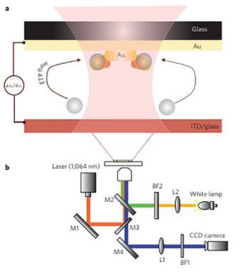
Image Caption: This image shows plasmonic nanotweezers for the lab-on-a-chip technology and the experimental setup used for excitation of the plasmonic nanostructure and imaging of the motion of suspended tracer particles.
The researchers developed a nanostructured plasmonic metafilm by perforating nanoscale holes in a gold film. Then, the metafilm acts as tweezers to capture and trap tiny particles by focusing light onto specific spots on the film and by heating up those spots and creating local thermal gradients in the ambient liquid. This produces a small tornado-like effect.
“All of this is resulting in a revolutionary compact lab-on-a-chip – an innovative approach to detecting and diagnosing a tumor or a viral disease,” said Alexander Kildishev, an associate professor with Purdue’s School of Electrical and Computer Engineering, who helped lead the research team.
The Purdue plasmonic metafilms use a combination of thermal and electric fields to create hydrodynamic flows that result in the rapid transport of suspended particles, bringing them to the surface of the metal film for easy trapping and detection.
Another advantage of the new system is the increased ability to sort these tiny particles and then collectively detect sorted patterns such as drug contaminants or water impurities. The technology has potential applications for pharmaceuticals, biohazard detection and water quality tests.
“To our knowledge, our plasmonic nanotweezers are more robust in trapping and detecting molecules than previous comparable lab-on-a-chip systems,” Kildishev said. “Our system also provides better sensitivity and consumes less laser power. We have created an advanced self-contained lab-on-a-chip platform that allows us to trap and detect dangerous particles such as drug and water contaminants and remove them from liquids.”
“Our system is very flexible to control and provides a broad range of functionality,” Kildishev said. “We use multifunctional, inexpensive light sources to outperform more expensive alternatives.”
The Purdue nanotweezers could be also used with these inexpensive broadband light sources for combining noble metal and dielectric nanoparticles, which could have applications for long-lasting, non-fading color printing.
Share on:


Testimonial
"The I-Connect007 team is outstanding—kind, responsive, and a true marketing partner. Their design team created fresh, eye-catching ads, and their editorial support polished our content to let our brand shine. Thank you all! "
Sweeney Ng - CEE PCBSuggested Items
Sensors: The Invisible Force Behind Modern Convenience and Safety
10/24/2025 | Sanjeev Mane, Brooks AutomationSensors and sensor technology are fundamental components of modern life that drive innovation across various electronics and devices. From smartphones to industrial machinery, these small but powerful tools enable seamless interaction with the environment, ensuring efficiency and safety. This article serves as an introduction and overview of sensor technology, highlighting its significance in modern applications and its growing importance in the market as we embrace smarter, more connected systems.
Technica USA Partners with Creative Electron
10/22/2025 | Technica USATechnica USA is proud to announce the partnership with Creative Electron Inc. located in San Marcos, CA.
MES Software Tools Need Thoughtful Integration
10/21/2025 | Nolan Johnson, SMT007 MagazineThe Global Electronics Association recently published a survey report on the state of EMS production software. This project, led by Thiago Guimaraes, director of industry intelligence, connects the dots across the global electronics value chain to uncover practical insights that individual companies might not have seen on their own. In this interview, Thiago discusses the whys and hows of this report.
Light-curable Solutions for Reliable Electronics in Space Applications
10/15/2025 | Virginia Hogan, DymaxDesigning electronics for space environments, particularly those in low Earth orbit (LEO), requires careful consideration of materials that can withstand extreme conditions while supporting long-term reliability. Engineers designing satellite systems, aerospace instrumentation, and high-altitude platforms face a familiar set of challenges: contamination control, mechanical stress, thermal cycling, and manufacturability.
Analog Devices Launches ADI Power Studio™ and New Web-Based Tools
10/14/2025 | Analog Devices, Inc.Analog Devices, Inc., a global semiconductor leader, announced the launch of ADI Power Studio, a comprehensive family of products that offers advanced modeling, component recommendations and efficiency analysis with simulation. In addition, ADI is introducing early versions of two new web-based tools with a modernized user experience under the Power Studio umbrella: