


 The Chemical Connection: Onshoring PCB Production—Daunting but Certainly Possible
 It’s Only Common Sense: The Phone Is Still Mightier Than the Keyboard


Two-Faced Edge Makes Nanotubes Obey
August 3, 2018 | Rice UniversityEstimated reading time: 5 minutes
Growing a batch of carbon nanotubes that are all the same may not be as simple as researchers had hoped, according to Rice University scientists.
Rice materials theorist Boris Yakobson and his team bucked a theory that when growing nanotubes in a furnace, a catalyst with a specific atomic arrangement and symmetry would reliably make carbon nanotubes of like chirality, the angle of its carbon-atom lattice.
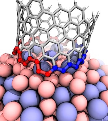
Image Caption: This illustration shows the interface between a growing carbon nanotube and a cobalt-tungsten catalyst. The atomic arrangement of the catalyst forces the nanotube to quickly transition from zigzag (blue) to armchair (red), which ultimately grows a nanotube that's neither one nor the other, but nearly in the middle. The transition is a previously undiscovered characteristic of carbon nanotube growth. (Credit: Evgeni Penev/Rice University)
Instead, they found the catalyst in question starts nanotubes with a variety of chiral angles but redirects almost all of them toward a fast-growing variant known as (12,6). The cause appears to be a Janus-like interface that is composed of armchair and zigzag segments – and ultimately changes how nanotubes grow.
Because chirality determines a nanotube’s electrical properties, the ability to grow chiral-specific batches is a nanotechnology holy grail. It could lead to wires that, unlike copper or aluminum, transmit energy without loss. Nanotubes generally grow in random chiralities.
The Rice theoretical study detailed in the American Chemical Society journal Nano Letters could be a step toward catalysts that produce homogenous batches of nanotubes, Yakobson said.
Yakobson and colleagues Evgeni Penev and Ksenia Bets and graduate student Nitant Gupta tackled a conundrum presented by other experimentalists at a 2013 workshop who used an alloy of cobalt and tungsten to catalyze single-walled nanotubes. In that lab’s batch, more than 90 percent of the nanotubes had a chirality of (12,6).
The numbers (12,6) are coordinates that refer to a nanotube’s chiral vector. Carbon nanotubes are rolled-up sheets of two-dimensional graphene. Graphene is highly conductive, but when it is rolled into a tube, its conductivity depends on the angle — or chirality — of its hexagonal lattice.
Armchair nanotubes — so called because of the armchair-like shape of their edges — have identical chiral indices, like (9,9), and are highly desired for their perfect conductivity. They are unlike zigzag nanotubes, such as (16,0), which may be semiconductors. Turning a graphene sheet a mere 30 degrees will change the nanotube it forms from armchair to zigzag or vice versa.
Penev said the experimentalists explained their work “in a way which was puzzling from the very beginning. They said this catalyst has a specific symmetry that matches the (12,6) edge, so these nanotubes preferentially nucleate and grow. This was the emergence of the so-called symmetry matching idea of carbon nanotube selective growth.
“We read and digested that, but we still couldn’t wrap our minds around it,” he said.
Shortly after the 2013 conference, the Yakobson lab published its own theory of nanotube growth, which showed that the balance between two opposing forces — the energy of the catalyst-nanotube contact and the speed at which atoms attach themselves to the growing tube at the interface — are responsible for chirality.
Rice University scientists have decoded the unusual growth characteristic of carbon nanotubes that start out as one chirality but switch to another, resulting in nearly homogenous batches of single-walled nanotubes. The nanotubes grow via chemical vapor deposition with a carbon-tungsten alloy catalyst. (Credit: Evgeni Penev/Rice University)
Page 1 of 2
Share on:


Testimonial
"Your magazines are a great platform for people to exchange knowledge. Thank you for the work that you do."
Simon Khesin - Schmoll MaschinenSuggested Items
Episode 6 of Ultra HDI Podcast Series Explores Copper-filled Microvias in Advanced PCB Design and Fabrication
10/15/2025 | I-Connect007I-Connect007 has released Episode 6 of its acclaimed On the Line with... American Standard Circuits: Ultra High Density Interconnect (UHDI) podcast series. In this episode, “Copper Filling of Vias,” host Nolan Johnson once again welcomes John Johnson, Director of Quality and Advanced Technology at American Standard Circuits, for a deep dive into the pros and cons of copper plating microvias—from both the fabricator’s and designer’s perspectives.
Nolan’s Notes: Tariffs, Technologies, and Optimization
10/01/2025 | Nolan Johnson -- Column: Nolan's NotesLast month, SMT007 Magazine spotlighted India, and boy, did we pick a good time to do so. Tariff and trade news involving India was breaking like a storm surge. The U.S. tariffs shifted India from one of the most favorable trade agreements to the least favorable. Electronics continue to be exempt for the time being, but lest you think that we’re free and clear because we manufacture electronics, steel and aluminum are specifically called out at the 50% tariff levels.
MacDermid Alpha & Graphic PLC Lead UK’s First Horizontal Electroless Copper Installation
09/30/2025 | MacDermid Alpha & Graphic PLCMacDermid Alpha Electronics Solutions, a leading supplier of integrated materials and chemistries to the electronics industry, is proud to support Graphic PLC, a Somacis company, with the installation of the first horizontal electroless copper metallization process in the UK.
Electrodeposited Copper Foils Market to Grow by $11.7 Billion Over 2025-2032
09/18/2025 | Globe NewswireThe global electrodeposited copper foils market is poised for dynamic growth, driven by the rising adoption in advanced electronics and renewable energy storage solutions.
MacDermid Alpha Showcases Advanced Interconnect Solutions at PCIM Asia 2025
09/18/2025 | MacDermid Alpha Electronics SolutionsMacDermid Alpha Electronic Solutions, a global leader in materials for power electronics and semiconductor assembly, will showcase its latest interconnect innovations in electronic interconnect materials at PCIM Asia 2025, held from September 24 to 26 at the Shanghai New International Expo Centre, Booth N5-E30