


 Trouble in Your Tank: Implementing Direct Metallization in Advanced Substrate Packaging
 It’s Only Common Sense: Storytelling That Sells—Stop Pitching, Start Painting Pictures
 The Right Approach: Get Ready for ISO 9001 Version 6


Two-Faced Edge Makes Nanotubes Obey
August 3, 2018 | Rice UniversityEstimated reading time: 5 minutes
Growing a batch of carbon nanotubes that are all the same may not be as simple as researchers had hoped, according to Rice University scientists.
Rice materials theorist Boris Yakobson and his team bucked a theory that when growing nanotubes in a furnace, a catalyst with a specific atomic arrangement and symmetry would reliably make carbon nanotubes of like chirality, the angle of its carbon-atom lattice.
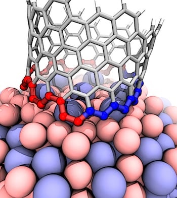
Image Caption: This illustration shows the interface between a growing carbon nanotube and a cobalt-tungsten catalyst. The atomic arrangement of the catalyst forces the nanotube to quickly transition from zigzag (blue) to armchair (red), which ultimately grows a nanotube that's neither one nor the other, but nearly in the middle. The transition is a previously undiscovered characteristic of carbon nanotube growth. (Credit: Evgeni Penev/Rice University)
Instead, they found the catalyst in question starts nanotubes with a variety of chiral angles but redirects almost all of them toward a fast-growing variant known as (12,6). The cause appears to be a Janus-like interface that is composed of armchair and zigzag segments – and ultimately changes how nanotubes grow.
Because chirality determines a nanotube’s electrical properties, the ability to grow chiral-specific batches is a nanotechnology holy grail. It could lead to wires that, unlike copper or aluminum, transmit energy without loss. Nanotubes generally grow in random chiralities.
The Rice theoretical study detailed in the American Chemical Society journal Nano Letters could be a step toward catalysts that produce homogenous batches of nanotubes, Yakobson said.
Yakobson and colleagues Evgeni Penev and Ksenia Bets and graduate student Nitant Gupta tackled a conundrum presented by other experimentalists at a 2013 workshop who used an alloy of cobalt and tungsten to catalyze single-walled nanotubes. In that lab’s batch, more than 90 percent of the nanotubes had a chirality of (12,6).
The numbers (12,6) are coordinates that refer to a nanotube’s chiral vector. Carbon nanotubes are rolled-up sheets of two-dimensional graphene. Graphene is highly conductive, but when it is rolled into a tube, its conductivity depends on the angle — or chirality — of its hexagonal lattice.
Armchair nanotubes — so called because of the armchair-like shape of their edges — have identical chiral indices, like (9,9), and are highly desired for their perfect conductivity. They are unlike zigzag nanotubes, such as (16,0), which may be semiconductors. Turning a graphene sheet a mere 30 degrees will change the nanotube it forms from armchair to zigzag or vice versa.
Penev said the experimentalists explained their work “in a way which was puzzling from the very beginning. They said this catalyst has a specific symmetry that matches the (12,6) edge, so these nanotubes preferentially nucleate and grow. This was the emergence of the so-called symmetry matching idea of carbon nanotube selective growth.
“We read and digested that, but we still couldn’t wrap our minds around it,” he said.
Shortly after the 2013 conference, the Yakobson lab published its own theory of nanotube growth, which showed that the balance between two opposing forces — the energy of the catalyst-nanotube contact and the speed at which atoms attach themselves to the growing tube at the interface — are responsible for chirality.
Rice University scientists have decoded the unusual growth characteristic of carbon nanotubes that start out as one chirality but switch to another, resulting in nearly homogenous batches of single-walled nanotubes. The nanotubes grow via chemical vapor deposition with a carbon-tungsten alloy catalyst. (Credit: Evgeni Penev/Rice University)
Page 1 of 2
Share on:


Testimonial
"The I-Connect007 team is outstanding—kind, responsive, and a true marketing partner. Their design team created fresh, eye-catching ads, and their editorial support polished our content to let our brand shine. Thank you all! "
Sweeney Ng - CEE PCBSuggested Items
Trouble in Your Tank: Implementing Direct Metallization in Advanced Substrate Packaging
09/15/2025 | Michael Carano -- Column: Trouble in Your TankDirect metallization systems based on conductive graphite are gaining popularity throughout the world. The environmental and productivity gains achievable with this process are outstanding. Direct metallization reduces the costs of compliance, waste treatment, and legal issues related to chemical exposure. A graphite-based direct plate system has been devised to address these needs.
Closing the Loop on PCB Etching Waste
09/09/2025 | Shawn Stone, IECAs the PCB industry continues its push toward greener, more cost-efficient operations, Sigma Engineering’s Mecer System offers a comprehensive solution to two of the industry’s most persistent pain points: etchant consumption and rinse water waste. Designed as a modular, fully automated platform, the Mecer System regenerates spent copper etchants—both alkaline and acidic—and simultaneously recycles rinse water, transforming a traditionally linear chemical process into a closed-loop system.
Driving Innovation: Depth Routing Processes—Achieving Unparalleled Precision in Complex PCBs
09/08/2025 | Kurt Palmer -- Column: Driving InnovationIn PCB manufacturing, the demand for increasingly complex and miniaturized designs continually pushes the boundaries of traditional fabrication methods, including depth routing. Success in these applications demands not only on robust machinery but also sophisticated control functions. PCB manufacturers rely on advanced machine features and process methodologies to meet their precise depth routing goals. Here, I’ll explore some crucial functions that empower manufacturers to master complex depth routing challenges.
Trouble in Your Tank: Minimizing Small-via Defects for High-reliability PCBs
08/27/2025 | Michael Carano -- Column: Trouble in Your TankTo quote the comedian Stephen Wright, “If at first you don’t succeed, then skydiving is not for you.” That can be the battle cry when you find that only small-diameter vias are exhibiting voids. Why are small holes more prone to voids than larger vias when processed through electroless copper? There are several reasons.
The Government Circuit: Navigating New Trade Headwinds and New Partnerships
08/25/2025 | Chris Mitchell -- Column: The Government CircuitAs global trade winds continue to howl, the electronics manufacturing industry finds itself at a critical juncture. After months of warnings, the U.S. Government has implemented a broad array of tariff increases, with fresh duties hitting copper-based products, semiconductors, and imports from many nations. On the positive side, tentative trade agreements with Europe, China, Japan, and other nations are providing at least some clarity and counterbalance.