


 The Chemical Connection: Onshoring PCB Production—Daunting but Certainly Possible
 It’s Only Common Sense: The Phone Is Still Mightier Than the Keyboard


Wearable ‘Microbrewery’ Saves Human Body from Radiation Damage
August 15, 2018 | Purdue UniversityEstimated reading time: 2 minutes
The same way that yeast yields beer and bread can help hospital lab workers better track their daily radiation exposure, enabling a faster assessment of tissue damage that could lead to cancer.
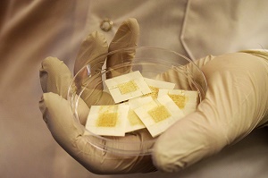
Image Caption: Workers in hospitals and nuclear facilities can wear disposable yeast badges to check their daily radiation exposure instantly. (Purdue University image/Kayla Wiles)
But rather than building portable cellars or ovens, Purdue University researchers have engineered yeast "microbreweries" within disposable badges made of freezer paper, aluminum and tape. Simply adding a drop of water activates the yeast to show radiation exposure as read by an electronic device.
On a commercial level, the readout device could one day be a tablet or phone. The badge could also be adapted in the future for nuclear power plant workers and victims of nuclear disasters.
"You would use the badge when you're in the lab and recycle it after you've checked your exposure by plugging it into a device," said Manuel Ochoa, a postdoctoral researcher in Purdue's School of Electrical and Computer Engineering.
Radiology workers are regularly exposed to low doses of radiation when they obtain patient imagery, such as X-rays. While protective gear largely keeps workers within a safe range of radiation exposure, absorbing a little bit is still inevitable.
Radiation doses creeping above regulated guidelines pose risk for developing conditions such as cancer, cataracts, skin irritation or thyroid disease.
"Currently, radiology workers are required to wear badges, called dosimeters, on various parts of their bodies for monitoring their radiation exposure," said Babak Ziaie, Purdue professor of electrical and computer engineering. "They wear the badges for a month or two, and then they send them to the company that made them. But it takes weeks for the company to read the data and send a report back to the hospital. Ours give an instant reading at much lower cost."
The success of the badge lies in the quick and measurable response of yeast to radiation: The higher the radiation dose, the higher the percentage of yeast cells that die. Wetting the badge activates the cells that are still alive to eat glucose and release carbon dioxide – the same fermentation process responsible for brewing beer and making bread rise.
When carbon dioxide bubbles at the surface, ions also form. The concentration of these ions increases the electrical conductivity of yeast, which can be measured by hooking up the badge to a readout system.
"We use the change in electrical properties of the yeast to tell us how much radiation damage it incurred. A slow decrease in electrical conductivity over time indicates more damage," said Rahim Rahimi, Purdue postdoctoral researcher in electrical and computer engineering.
Numbers from the readout system translate to rads – the units used by entities like the Occupational Safety and Health Administration to specify limits on how much radiation human tissue can safely absorb. Skin of the whole body, for example, shouldn't be exposed to more than 7.5 rad over a three month period.
The researchers could detect a radiation dose as little as 1 millirad in the yeast badges, which is comparable to current commercial badges.
Yeast also is known to be genetically similar to human tissue. Data from the badges can, therefore, inform future work on how radiation damage happens to human DNA and proteins.
"For yeast, it seems that radiation primarily affects the cell walls of the membrane and mitochondria," Ochoa said. "Since biologists are already familiar with yeast, then we're more likely to understand what's causing the biological effects of radiation in organic matter."
Share on:


Testimonial
"Our marketing partnership with I-Connect007 is already delivering. Just a day after our press release went live, we received a direct inquiry about our updated products!"
Rachael Temple - AlltematedSuggested Items
Zuken Announces ZIW Americas 2026 in Dallas
10/21/2025 | ZukenZuken USA, Inc., a global leader in electrical and electronic design automation, announced Zuken Innovation World (ZIW) Americas 2026, the company’s premier global conference dedicated to advancing the future of electrical and electronic product design. ZIW 2026 will be held June 9-11 in Dallas, Texas.
ITW EAE Despatch Ovens Now Support ASTM 5423 Testing
10/15/2025 | ITW EAEAs the demand for high-performance electrical insulation materials continues to grow—driven by the rapid expansion of electric vehicles (EVs) and energy storage systems—thermal processing has become a critical step in material development.
Target Condition: Floor Planning Without a Floor
08/27/2025 | Kelly Dack -- Column: Target ConditionBy a show of hands, how many PCB designers have been asked to start a layout without a board outline, keep-out zones, or even height constraints? How many have had to work within a specific enclosure before the schematic was finalized? If this sounds familiar, you're not alone. Starting a PCB layout without critical constraints is like hiring an interior designer to buy furniture and carpet for a house you haven’t even purchased yet, or, even worse, trying to fit four bedrooms' worth of furniture in a one-room cabin.
Indium Joins Virginia Tech Center for Power Electronics Systems Industry Consortium
06/03/2025 | Indium CorporationIndium Corporation®, a leading materials refiner, smelter, manufacturer, and supplier to the global electronics, semiconductor, thin-film, and thermal management markets, has joined Virginia Tech’s Center for Power Electronics Systems (CPES), an industry consortium that supports power electronics initiatives to reduce energy use while growing capability.
IPC Launches New Wire Harness Design Course Led by Defense Industry Expert
06/03/2025 | I-Connect007 Editorial TeamIPC is expanding its educational offerings with a new online course designed to provide foundational knowledge in wire harness and cable design. The course, Introduction to Wire Harness Design I, is led by a seasoned mechanical engineer and subject matter expert in military cable systems working at FNSS Defense Systems in Turkey.