


 American Made Advocacy: Smart Policies Can Ensure AI Data Centers Are Secure
 Beyond the Board: Early Engagement Means Faster Prototyping for Defense Programs
 Defense Speak Interpreted: The Autonomous Plane Battle—Skyborg Vs. Loyal Wingman


MIRTEC Enters Tech Collaboration Agreement with YXLON and The Comet Group
August 20, 2018 | MirtecEstimated reading time: 2 minutes
MIRTEC has entered into a technical collaboration agreement with YXLON, a company of the Comet Group. This collaboration allows both organizations to explore and expand upon synergistic applications within the SMT electronics manufacturing industry.
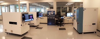
Pictured above, MIRTEC and YXLON equipment are on display at the Comet Group Lab ONE facility in San Jose, California. This new ‘Center of Excellence’ gives customers the opportunity to enjoy hands-on experience and demonstrations with MIRTEC’s latest solder paste inspection (SPI) and automated optical inspection (AOI) Systems in conjunction with YXLON’s state-of-the-art Automated x-ray inspection (AXI) technology. These systems are fully integrated with the SmartLoop yield improvement system.
MIRTEC, together with YXLON, have delivered a game-changing Industry 4.0 solution. SmartLoop links MIRTEC’s in-line 3D AOI with the YXLON’s at-line digital x-ray system, allowing data to flow between them seamlessly.
“3D AOI can only measure differences in Z-height on devices like BGAs and make a guestimate as to the quality of the joints underneath and the need for rework. With SmartLoop, the at-line x-ray system now becomes a verification station for the 3D height measurements taken by the AOI system. X-Ray inspection time is also dramatically reduced by targeting only suspect regions of interest that the system automatically selects for inspection. Full data integration gives the technician the tools needed for correct decisions, intelligent feedback and process improvements,” said Keith Bryant, YXLON global director of electronics sales.
“We are very excited to partner with YXLON and the Comet Group. Our intention is to collaborate on new inspection solutions for the Electronic Manufacturing Industry, combining the strengths of MIRTEC’s Award Winning 3D Inspection Technology with YXLON International’s advanced X-ray and CT inspection systems. These new solutions will provide our valued customers with leading-edge inspection capabilities required in the production of complex electronic assemblies and help pave the way toward Industry 4.0 through collaborative data integration. We look forward to a long and prosperous relationship between our organizations,” said Brian D’Amico, president of MIRTEC’s North American Sales and Service Division.
About MIRTEC
MIRTEC has earned a solid reputation with leading OEM and EMS companies throughout the world for its technologically advanced 3D inspection technology. MIRTEC products have been extremely successful in high-volume markets including cell phone and MP3 player manufacturing, as well as low-volume high-mix markets such as medical, automotive, aerospace and defense. For more information, click here.
About YXLON
YXLON, company of the Comet Group, designs and produces radioscopic and CT inspection systems for a broad variety of industrial applications and fields. Whether in the aviation and aerospace, automotive, or electronics industry, YXLON customers are among the largest manufacturers in the world. For more information, click here.
About COMET Group
The COMET Group is a globally leading, innovative Swiss technology company with a focus on the x-ray, radio frequency and ebeam businesses. With premium high-tech components and systems, we enable customers in numerous industries to both enhance the quality of their products and make their manufacturing more efficient and eco-friendly. Our innovative solutions under the COMET, YXLON and ebeam brands are in demand for applications such as materials testing and security inspection, the coating and treatment of surfaces, and non-contact sterilization. Based in Flamatt, Switzerland, the COMET Group has a presence in all world markets. We employ about 1,300 people worldwide, including approximately 440 in Switzerland. Besides production facilities in China, Denmark, Germany, Switzerland and the USA, we maintain various subsidiaries in the USA, China, Japan and Korea. COMET’s stock (COTN) is listed on the SIX Swiss Exchange. For more information, click here.
Share on:


Testimonial
"Advertising in PCB007 Magazine has been a great way to showcase our bare board testers to the right audience. The I-Connect007 team makes the process smooth and professional. We’re proud to be featured in such a trusted publication."
Klaus Koziol - atgSuggested Items
BTU International Earns 2025 Step-by-Step Excellence Award for Its Aqua Scrub™ Flux Management System
10/29/2025 | BTU International, Inc.BTU International, Inc., a leading supplier of advanced thermal processing equipment for the electronics manufacturing market, has been recognized with a 2025 Step-by-Step Excellence Award (SbSEA) for its Aqua Scrub™ Flux Management Technology, featured on the company’s Pyramax™ and Aurora™ reflow ovens.
On the Line With… Ultra HDI Podcast—Episode 7: “Solder Mask: Beyond the Traces,” Now Available
10/31/2025 | I-Connect007I-Connect007 is excited to announce the release of the seventh episode of its 12-part podcast series, On the Line With… American Standard Circuits: Ultra HDI. In this episode, “Solder Mask: Beyond the Traces,” host Nolan Johnson sits down with John Johnson, Director of Quality and Advanced Technology at American Standard Circuits, to explore the essential role that solder mask plays in the Ultra HDI (UHDI) manufacturing process.
Rehm Wins Mexico Technology Award for CondensoXLine with Formic Acid
10/17/2025 | Rehm Thermal SystemsModern electronics manufacturing requires technologies with high reliability. By using formic acid in convection, condensation, and contact soldering, Rehm Thermal Systems’ equipment ensures reliable, void-free solder joints — even when using flux-free solder pastes.
Indium Experts to Deliver Technical Presentations at SMTA International
10/14/2025 | Indium CorporationAs one of the leading materials providers to the power electronics assembly industry, Indium Corporation experts will share their technical insight on a wide range of innovative solder solutions at SMTA International (SMTAI), to be held October 19-23 in Rosemont, Illinois.
Knocking Down the Bone Pile: Revamp Your Components with BGA Reballing
10/14/2025 | Nash Bell -- Column: Knocking Down the Bone PileBall grid array (BGA) components evolved from pin grid array (PGA) devices, carrying over many of the same electrical benefits while introducing a more compact and efficient interconnect format. Instead of discrete leads, BGAs rely on solder balls on the underside of the package to connect to the PCB. In some advanced designs, solder balls are on both the PCB and the BGA package. In stacked configurations, such as package-on-package (PoP), these solder balls also interconnect multiple packages, enabling higher functionality in a smaller footprint.