


 Beyond the Board: Early Engagement Means Faster Prototyping for Defense Programs
 Defense Speak Interpreted: The Autonomous Plane Battle—Skyborg Vs. Loyal Wingman
 American Made Advocacy: Congress Back from Break With Work To Do


Shen's Spectacular Supersolder
August 22, 2018 | Carnegie Mellon UniversityEstimated reading time: 3 minutes
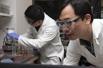
Carnegie Mellon University's Sheng Shen has created a solder-like material called supersolder, with twice the thermal conductivity of conventional solders and a compliance higher by two to three orders of magnitude.
In electronics, solder is used to connect two parts together. As a bridge, one of its most important functions is to transfer heat away from critical electronic components and toward the heat sink, which uses air or water to safely dissipate heat. As technological advances allow for the creation of smaller and more powerful computers and electronics — and with temperatures in computer chips reaching higher than 100°C — this heat dissipation function has become more crucial than ever.
Conventional solders are limited in their ability to conduct heat effectively over a long lifetime, making heat dissipation an obstacle for further computing and electronics development. If these fields are to advance further, this crucial bottleneck will have to be overcome.
The supersolder assembly, consisting of a layer of copper and tin nanowires sandwiched between two pieces of silicon to simulate the two parts being connected.
The product of a 2013 DARPA Young Faculty Award, supersolder is a thermal interface material developed by Shen, an associate professor of mechanical engineering, in collaboration with researchers from the National Renewable Energy Laboratory. Four years of work have resulted in the creation of a material that can fill the same role as conventional solders but with twice the thermal conductance of current state-of-the-art thermal interface materials.
The secret behind Shen's breakthrough is copper-tin nanowire arrays.
"The nanowires are grown from a template, like a mold, using small pores," Shen said. "It's chip technology using electroplating, grown one layer at a time, like how you coat an electrical cord by dipping it into electrolyte."
The resulting array exhibits remarkable thermal properties, unparalleled by any current solder materials. It's not just its thermal conductance that makes supersolder unique.
Supersolder also exhibits extraordinary compliance, or elasticity, on par with that of rubber or other polymers. This is important, as the parts that the solder connects expand and contract when heated, often at varying rates between two parts of differing composition. Diminishing compliance is often the downfall of conventional solders, as they grow brittle over repeated use, degrading their ability to conduct heat over time. According to Shen, supersolder's compliance is higher than these materials by two to three orders of magnitude.
An experiment his team conducted matched a supersolder assembly against a conventional solder assembly of tin. While the conventional solder began to decline in thermal conductance after less than 300 hours of cycling, the supersolder continued to operate at peak thermal conductance after more than 600 hours. In fact, it performed so well that its exact limits are unknown.
"We know it can keep going," Shen said. "The only reason we ended the experiment was because we had to publish the paper!"
Supersolder could replace conventional solder in electronic systems ranging from micro- and portable electronics to warehouse-sized data centers, reducing temperatures to enable significant improvements in power density and reliability. Anything conventional solder can do, supersolder can do better - almost.
While Shen is very pleased with the results from supersolder, he still sees room for improvement. The material is electrically conductive: an attribute that is undesirable in certain applications. His next goal is to create a version of supersolder that can retain its thermal conductance while acting as an electrical insulator.
After four years of work, there is little that could deter him from perfecting his material.
"The idea is very simple: you have a challenge, and you keep trying until you make it work," he said.
Mechanical Engineering faculty member Sheng Shen describes his work developing low-density, multi-functional materials that have a broad range of applications in aerospace, automotive, and biomedical technologies.
Share on:


Testimonial
"Our marketing partnership with I-Connect007 is already delivering. Just a day after our press release went live, we received a direct inquiry about our updated products!"
Rachael Temple - AlltematedSuggested Items
Rehm Wins Mexico Technology Award for CondensoXLine with Formic Acid
10/17/2025 | Rehm Thermal SystemsModern electronics manufacturing requires technologies with high reliability. By using formic acid in convection, condensation, and contact soldering, Rehm Thermal Systems’ equipment ensures reliable, void-free solder joints — even when using flux-free solder pastes.
Indium Experts to Deliver Technical Presentations at SMTA International
10/14/2025 | Indium CorporationAs one of the leading materials providers to the power electronics assembly industry, Indium Corporation experts will share their technical insight on a wide range of innovative solder solutions at SMTA International (SMTAI), to be held October 19-23 in Rosemont, Illinois.
Knocking Down the Bone Pile: Revamp Your Components with BGA Reballing
10/14/2025 | Nash Bell -- Column: Knocking Down the Bone PileBall grid array (BGA) components evolved from pin grid array (PGA) devices, carrying over many of the same electrical benefits while introducing a more compact and efficient interconnect format. Instead of discrete leads, BGAs rely on solder balls on the underside of the package to connect to the PCB. In some advanced designs, solder balls are on both the PCB and the BGA package. In stacked configurations, such as package-on-package (PoP), these solder balls also interconnect multiple packages, enabling higher functionality in a smaller footprint.
Indium to Showcase High-Reliability Solder and Flux-Cored Wire Solutions at SMTA International
10/09/2025 | Indium CorporationAs one of the leading materials providers in the electronics industry, Indium Corporation® will feature its innovative, high-reliability solder and flux-cored wire products at SMTA International (SMTAI), to be held October 19-23 in Rosemont, Illinois.
‘Create your Connections’ – Rehm at productronica 2025 in Munich
10/08/2025 | Rehm Thermal SystemsThe electronics industry is undergoing dynamic transformation: smart production lines, sustainability, artificial intelligence, and sensor technologies dominate current discussions.