


 Driving Innovation: Mechanical and Optical Processes During Rigid-flex Production
 It’s Only Common Sense: Your Biggest Competitor Is Complacency
 The Chemical Connection: Onshoring PCB Production—Daunting but Certainly Possible


Printing Solar Cells and Organic LEDs
August 23, 2018 | HZBEstimated reading time: 2 minutes
Humboldt-Universität zu Berlin and Helmholtz-Zentrum Berlin form a joint lab and research group “Generative production processes for hybrid components”.
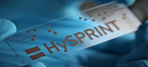
Image Caption: The HySPRINT logo (Helmholtz Innovation Lab) printed on a copper solution symbolizes how the thinnest material layers can be produced simply and cost-effectively. Possible applications are solar cells, organic LEDs or transistors. Photo credit: Humboldt Universität zu Berlin/List-Kratochvil
Solar cells, LEDs and detectors made of organic and hybrid semiconductors can nowadays be simply printed out, even together with teensy nanostructures that make them function better. The development of low-cost printing methods for electronic and optoelectronic components is at the centre of things for the new joint research group and the joint laboratory of the Helmholtz-Zentrum Berlin (HZB) and Humboldt-Universität zu Berlin (HU).
Cooperating together in the new research group are the HU workgroup “Hybrid Devices” led by Prof. Dr. Emil List-Kratochvil, the HZB young investigator group of Dr. Eva Unger, the Helmholtz Innovation Lab HySPRINT, and the Competence Centre Photovoltaics Berlin (PVcomB) directed by Prof. Dr. Rutger Schlatmann. The partners are building up a joint lab at Humboldt-Universität zu Berlin that will allow the researchers to acquire and use complementary laboratory infrastructures for various coating methods.
Prof. Emil List-Kratochvil is the head of the HU workgroup “Hybrid Devices” at IRIS Adlershof, and has been working for 15 years on developing electronic and optoelectronic hybrid components, resource-efficient deposition techniques (inkjet printing) and in-situ nanostructuring and synthetic methods. This expertise complements the aims of the HZB young investigator group led by Dr. Eva Unger. She will be developing solution-based manufacturing methods for depositing perovskite semiconductor layers onto larger surface areas for solar cells. “The new research group with List-Kratochvil is a real win for us. With his experience in printed electronic components, he is an ideal cooperation partner for us,” Unger says.
In recent months, the researcher and her team have already come much closer to her goal of developing hybrid tandem solar cells with large-surface-areas in the scope of the Helmholtz Innovation Lab HySPRINT. Now, the next step is to upscale the process in order to drive the novel solar cells towards market maturity. The Competence Centre Thin-Film- and Nanotechnology for Photovoltaics Berlin (PVcomB) is the ideal partner for the development of industrially relevant manufacturing processes. The joint research group is now striving towards building a pilot line on which to develop prototypes of hybrid components.
Share on:


Testimonial
"The I-Connect007 team is outstanding—kind, responsive, and a true marketing partner. Their design team created fresh, eye-catching ads, and their editorial support polished our content to let our brand shine. Thank you all! "
Sweeney Ng - CEE PCBSuggested Items
WestDev Announces Advanced Thermal Analysis Integration for Pulsonix PCB Design Suite
10/29/2025 | WestDev Ltd.Pulsonix, the industry-leading PCB design software from WestDev Ltd., announced a major enhancement to its design ecosystem: a direct interface between Pulsonix and ADAM Research's TRM (Thermal Risk Management) analysis software.
Designers Notebook: Power and Ground Distribution Basics
10/29/2025 | Vern Solberg -- Column: Designer's NotebookThe principal objectives to be established during the planning stage are to define the interrelationship between all component elements and confirm that there is sufficient surface area for placement, the space needed to ensure efficient circuit interconnect, and to accommodate adequate power and ground distribution.
Episode 6 of Ultra HDI Podcast Series Explores Copper-filled Microvias in Advanced PCB Design and Fabrication
10/15/2025 | I-Connect007I-Connect007 has released Episode 6 of its acclaimed On the Line with... American Standard Circuits: Ultra High Density Interconnect (UHDI) podcast series. In this episode, “Copper Filling of Vias,” host Nolan Johnson once again welcomes John Johnson, Director of Quality and Advanced Technology at American Standard Circuits, for a deep dive into the pros and cons of copper plating microvias—from both the fabricator’s and designer’s perspectives.
Nolan’s Notes: Tariffs, Technologies, and Optimization
10/01/2025 | Nolan Johnson -- Column: Nolan's NotesLast month, SMT007 Magazine spotlighted India, and boy, did we pick a good time to do so. Tariff and trade news involving India was breaking like a storm surge. The U.S. tariffs shifted India from one of the most favorable trade agreements to the least favorable. Electronics continue to be exempt for the time being, but lest you think that we’re free and clear because we manufacture electronics, steel and aluminum are specifically called out at the 50% tariff levels.
MacDermid Alpha & Graphic PLC Lead UK’s First Horizontal Electroless Copper Installation
09/30/2025 | MacDermid Alpha & Graphic PLCMacDermid Alpha Electronics Solutions, a leading supplier of integrated materials and chemistries to the electronics industry, is proud to support Graphic PLC, a Somacis company, with the installation of the first horizontal electroless copper metallization process in the UK.