


 Driving Innovation: Mechanical and Optical Processes During Rigid-flex Production
 It’s Only Common Sense: Your Biggest Competitor Is Complacency
 The Chemical Connection: Onshoring PCB Production—Daunting but Certainly Possible


Nano-Imaging of Intersubband Transitions in Few-Layer 2D Materials
August 28, 2018 | ICFOEstimated reading time: 2 minutes
A study in Nature Nanotechnology reports on the first observation of intersubband transitions in 2D materials via scattering scanning near-field optical microscopy. Semiconducting heterostructures have been key to the development of electronics and opto-electronics.
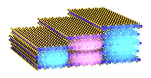
Image Caption: Schematic illustration of charge carriers confined within a TMD flake comprising different thicknesses. Charge carriers in the ground state (blue) can be excited upon resonant light excitation to a high.
Many applications in the infrared and terahertz frequency range exploit transitions, called intersubband transitions, between quantized states in semiconductor quantum wells. These intraband transitions exhibit very large oscillator strengths, close to unity. Their discovery in III-V semiconductor heterostructures depicted a huge impact within the condensed matter physics community and triggered the development of quantum well infrared photodetectors as well as quantum cascade lasers.
Quantum wells of the highest quality are typically fabricated by molecular beam epitaxy (sequential growth of crystalline layers), which is a well-established technique. However, it poses two major limitations: Lattice-matching is required, restricting the freedom in materials to choose from, and the thermal growth causes atomic diffusion and increases interface roughness. 2D materials can overcome these limitations since they naturally form a quantum well with atomically sharp interfaces. They provide defect free and atomically sharp interfaces, enabling the formation of ideal QWs, free of diffusive inhomogeneities. They do not require epitaxial growth on a matching substrate and can therefore be easily isolated and coupled to other electronic systems such as Si CMOS or optical systems such as cavities and waveguides.
Surprisingly enough, intersubband transitions in few-layer 2D materials had never been studied before, neither experimentally nor theoretically. Thus, in a recent study published in Nature Nanotechnology, ICFO researchers Peter Schmidt, Fabien Vialla, Mathieu Massicotte, Klaas-Jan Tielrooij, Gabriele Navickaite, led by ICREA Prof at ICFO Frank Koppens, in collaboration with the Institut Lumière Matière - CNRS, Technical University of Denmark, Max Planck Institute for the Structure and Dynamics of Matter, CIC nanoGUNE, and the National Graphene Institute, report on the first theoretical calculations and first experimental observation of inter-sub-band transitions in quantum wells of few-layer semiconducting 2D materials (TMDs).
In their experiment, the team of researchers applied scattering scanning near-field optical microscopy (s-SNOM) as an innovative approach for spectral absorption measurements with a spatial resolution below 20 nm. They exfoliated TMDs, which comprisedterraces of different layer thicknesses over lateral sizes of about a few micrometers. They directly observed the intersubband resonances for these different quantum well thicknesses within a single device. They also electrostatically tuned the charge carrier density and demonstrated intersubband absorption in both the valence and conduction band. These observations were complemented and supported with detailed theoretical calculations revealing many-body and non-local effects.
The results of this study pave the way towards an unexplored field in this new class of materials and offer a first glimpse of the physics and technology enabled by intersubband transitions in 2D materials, such as infrared detectors, sources, and lasers with the potential for compact integration with Si CMOS.
Share on:


Testimonial
"In a year when every marketing dollar mattered, I chose to keep I-Connect007 in our 2025 plan. Their commitment to high-quality, insightful content aligns with Koh Young’s values and helps readers navigate a changing industry. "
Brent Fischthal - Koh YoungSuggested Items
Sealed for Survival: Potting Electronics for the Toughest Environments
10/29/2025 | Beth Massey, MacDermid Alpha Electronics SolutionsElectronics deployed in harsh conditions face relentless threats from vibration, impact, chemical contaminants, airborne pollutants, and moisture, conditions that can quickly lead to failure without robust protection. Potting, the process of encapsulating electronics in a protective polymer, is a widely used strategy to safeguard devices from both environmental and mechanical hazards.
Driving Innovation: Mechanical and Optical Processes During Rigid-flex Production
10/28/2025 | Kurt Palmer -- Column: Driving InnovationRigid-flex printed circuit boards are a highly effective solution for placing complex circuitry in tight, three-dimensional spaces. They are now indispensable across a range of industries, from medical devices and aerospace to advanced consumer electronics, helping designers make the most efficient use of available space. However, their unique construction—combining rigid and flexible materials—presents a fundamental challenge for PCB manufacturers.
SMTAI 2025 Review: Reflecting on a Pragmatic and Forward-looking Industry
10/27/2025 | Marcy LaRont, I-Connect007Leaving the show floor on the final afternoon of SMTA International last week in Rosemont, Illinois, it was clear that the show remains a grounded, technically driven event that delivers a solid program, good networking, and an easy space to commune with industry colleagues and meet with customers.
ITW EAE Despatch Ovens Now Support ASTM 5423 Testing
10/15/2025 | ITW EAEAs the demand for high-performance electrical insulation materials continues to grow—driven by the rapid expansion of electric vehicles (EVs) and energy storage systems—thermal processing has become a critical step in material development.
Beyond Thermal Conductivity: Exploring Polymer-based TIM Strategies for High-power-density Electronics
10/13/2025 | Padmanabha Shakthivelu and Nico Bruijnis, MacDermid Alpha Electronics SolutionsAs power density and thermal loads continue to increase, effective thermal management becomes increasingly important. Rapid and efficient heat transfer from power semiconductor chip packages is essential for achieving optimal performance and ensuring long-term reliability of temperature-sensitive components. This is particularly crucial in power systems that support advanced applications such as green energy generation, electric vehicles, aerospace, and defense, along with high-speed computing for data centers and artificial intelligence (AI).