


 The Marketing Minute: If Your Marketing Budget Gets Cut in Half, Then What?
 Punching Out: How Are the Big Boys in Electronics Doing?
 It’s Only Common Sense: Complexity Is the Enemy of Profit


Atotech to Exhibit and Present at the SEMICON Taiwan Show
August 30, 2018 | AtotechEstimated reading time: 2 minutes
Atotech will participate at this year’s SEMICON Taiwan Show, held from September 5 to 7, 2018, in the Taipei Nangang Exhibition Center Hall 1 in Taipei, Taiwan. The Atotech team can be found at booth J2340 and at the SiP Global Summit where Dr. Ralf Schmidt, R&D Manager Semiconductor at Atotech Group, will exemplify the company’s answer for enhanced reliability of sub 5 µm L/S RDL for 5G.
“Next generation devices for FOWLP require the reduction of the RDL pitch to 1x1 µm or less. This leads to an increased importance of the mechanical properties. Recent findings point out the importance of the formation of a proper composite with the subjacent substrate, i.e. polyimide (PI). The composite formation can strongly improve the mechanical properties and, thus, the reliability of the Cu lines,” states Ralf.
In his presentation on Thursday, September 6, 2018, from 3:45 pm to 4:15 pm, Ralf will discuss the different solutions to promote the formation of a proper composite material consisting of Cu RDL lines and PI, especially with respect to their influence on mechanical properties as well as their suitability for potential 5G applications. The combination of high purity Cu deposits and strong composite formations with the substrate is considered to be a key parameter for future sub 5 µm L/S multilayer RDL technologies.
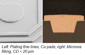
The company also announced a special product feature on Spherolyte UF3, a new wet chemical process solution for next generation RDLs in FOWLP, and MultiPlate, the company's new production tool for the simultaneous copper deposition for embedded power chips, at booth number J2340.
Spherolyte UF3
This product allows for fine line RDL plating and microvia filling in one process. Advantages include the low internal stress of less than 20 MPa and the low incorporation level of additives which enables high purity Cu deposits. Spherolyte UF3 also reduces Cu line breakages after thermal cycle testing.
MultiPlate for Power ICs
MultiPlate for power ICs was developed for the simultaneous copper deposition for embedding power chips and backside metallization. The Atotech tool allows for plating on 150, 200 and 300 mm wafers including Taiko thin wafers and panel sizes of up to 600 x 600 mm. The dual side metallization process minimizes warpage and enables high deposition uniformity at high plating speeds. This leads to a process cost reduction of up to 26 percent, and reduces the number of process steps by 25 percent, as compared to sequential processing.
About Atotech
Atotech is one of the world’s leading manufacturers of specialty chemicals and equipment for the printed circuit board, IC-substrate and semiconductor industries, as well as for the decorative and functional surface finishing industries. Atotech has annual sales of $1.2 billion (2017). The company is fully committed to sustainability – we develop technologies to minimize waste and to reduce environmental impact. Atotech has its headquarters in Berlin, Germany, and employs about 4,000 people in over 40 countries. For more information, click here.
Share on:


Testimonial
"The I-Connect007 team is outstanding—kind, responsive, and a true marketing partner. Their design team created fresh, eye-catching ads, and their editorial support polished our content to let our brand shine. Thank you all! "
Sweeney Ng - CEE PCBSuggested Items
I-Connect007 Releases The Printed Circuit Designer’s Guide to… Direct Metallization: A Guide to Complex PCB Fabrication
05/15/2026 | I-Connect007As PCB complexity continues to accelerate, fabricators and OEMs are reevaluating long-standing manufacturing processes to meet the demands of AI, HDI, advanced packaging, and next-generation electronics. To address these evolving challenges, I-Connect007 is proud to announce the release of The Printed Circuit Designer’s Guide to… Direct Metallization: A Guide to Complex PCB Fabrication, authored by MacDermid Alpha Solution’s Carmichael Gugliotti.
Driving Innovation: Selecting the Right Laser Source
04/28/2026 | Simon Khesin -- Column: Driving InnovationWhen I first joined Schmoll Maschinen, I brought experience from almost every PCB process, except for laser. As I immersed myself in laser processing, I realized why it can seem so daunting to a newcomer. The complexity arises from three intersecting factors: A vast variety of laser sources: CO2, UV-nano, green-pico, UV-pico, IR-pico, and others; a diverse range of applications: Drilling, cutting, ablation, and more; and an extensive list of materials: These have vastly different absorption rates. Choosing the right machine or laser source is rarely trivial. Even for experienced engineers, answering "Which source is best?" requires examining the business's specific goals.
Institute of Circuit Technology Spring Seminar 2026: A Bright Future in Europe
04/23/2026 | Pete Starkey, I-Connect007Through the leafy lanes and spring flowers of Warwickshire and back to Meridan, the traditional centre of England, and now officially part of the Metropolitan Borough of Solihull in the county of the West Midlands, I attended the Annual General Meeting and Spring Seminar of the Institute of Circuit Technology (ICT) on April 14. Out of the AGM came notable changes in leadership at the top of the Institute: the retirement of Mat Beadel as chair and Emma Hudson as technical director. Effective May 1, Steve Driver is the new chair, and Alun Morgan is the new technical director.
ACCM Unveils Negative and Near-zero CTE Materials for Large-Format AI Chips
04/21/2026 | Advanced Chip and Circuit MaterialsAdvanced Chip and Circuit Materials, Inc. (ACCM) has launched two new materials: Celeritas HM50, with a negative coefficient of thermal expansion (CTE) of -8 ppm/°C to offset the positive CTE and expansion of copper with temperature on circuit boards, and Celeritas HM001, with near-zero CTE and the low-loss performance needed for high-speed signal layers to 224 Gb/s and faster in artificial intelligence (AI) circuits.
Fresh PCB Concepts: Designing PCBs for Harsh Environments—Reliability Is Engineered Upstream
04/23/2026 | Team NCAB -- Column: Fresh PCB ConceptsWhen engineers hear the phrase “harsh environment,” they usually think of the extreme temperature swings, vibration and shock, pressure changes, or radiation in aerospace. However, aerospace is not the only harsh environment where electronic assemblies must survive. Automotive power electronics, downhole oil and gas tools, marine controls, rail systems, defense platforms, and industrial automation equipment all expose PCBs to environments that are equally unforgiving. The stress mechanisms may differ, but the physics does not.