


 Driving Innovation: Mechanical and Optical Processes During Rigid-flex Production
 It’s Only Common Sense: Your Biggest Competitor Is Complacency
 The Chemical Connection: Onshoring PCB Production—Daunting but Certainly Possible


Probing Individual Edge States With Unprecedented Precision
September 12, 2018 | University of BaselEstimated reading time: 2 minutes
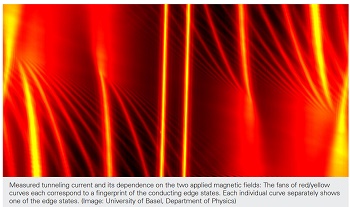
A new technique makes it possible to obtain an individual fingerprint of the current-carrying edge states occurring in novel materials such as topological insulators or 2D materials.
While insulators do not conduct electrical currents, some special materials exhibit peculiar electrical properties: though not conducting through their bulk, their surfaces and edges may support electrical currents due to quantum mechanical effects, and do so even without causing losses.
Such so-called topological insulators have attracted great interest in recent years due to their remarkable properties. In particular, their robust edge states are very promising since they could lead to great technological advances.
Currents Flowing Only Along the Edges
Similar effects as the edge states of such topological insulators also appear when a two-dimensional metal is exposed to a strong magnetic field at low temperatures. When the so-called quantum Hall effect is realized, current is thought to flow only at the edges, where several conducting channels are formed.
Probing Individual Edge States
Until now, it was not possible to address the numerous current carrying states individually or to determine their positions separately. The new technique now makes it possible to obtain an exact fingerprint of the current carrying edge states with nanometer resolution.
This is reported by researchers of the Department of Physics and the Swiss Nanoscience Institute of the University of Basel in collaboration with colleagues of the University of California, Los Angeles, as well as of Harvard and Princeton University, USA.
In order to measure the fingerprint of the conducting edge states, the physicists lead by Prof. Dominik Zumbühl have further developed a technique based on tunneling spectroscopy.
They have used a gallium arsenide nanowire located at the sample edge which runs in parallel to the edge states under investigation. In this configuration, electrons may jump (tunnel) back and forth between a specific edge state and the nanowire as long as the energies in both systems coincide. Using an additional magnetic field, the scientists control the momentum of tunneling electrons and can address individual edge states. From the measured tunneling currents, the position and evolution of each edge state may be obtained with nanometer precision.
Tracking the Evolution
This new technique is very versatile and can also be used to study dynamically evolving systems. Upon increasing the magnetic field, the number of edge states is reduced, and their distribution is modified. For the first time, the scientists were able to watch the full edge state evolution starting from their formation at very low magnetic fields.
With increasing magnetic field, the edge states are first compressed towards the sample boundary until eventually, they move towards the inside of the sample and then disappear completely. Analytical and numerical models developed by the research team agree very well with the experimental data.
“This new technique is not only very useful to study the quantum Hall edge states,” Dominik Zumbühl comments the results of the international collaboration. “It might also be employed to investigate new exotic materials such as topological insulators, graphene or other 2D materials.”
Share on:


Testimonial
"The I-Connect007 team is outstanding—kind, responsive, and a true marketing partner. Their design team created fresh, eye-catching ads, and their editorial support polished our content to let our brand shine. Thank you all! "
Sweeney Ng - CEE PCBSuggested Items
Sealed for Survival: Potting Electronics for the Toughest Environments
10/29/2025 | Beth Massey, MacDermid Alpha Electronics SolutionsElectronics deployed in harsh conditions face relentless threats from vibration, impact, chemical contaminants, airborne pollutants, and moisture, conditions that can quickly lead to failure without robust protection. Potting, the process of encapsulating electronics in a protective polymer, is a widely used strategy to safeguard devices from both environmental and mechanical hazards.
Driving Innovation: Mechanical and Optical Processes During Rigid-flex Production
10/28/2025 | Kurt Palmer -- Column: Driving InnovationRigid-flex printed circuit boards are a highly effective solution for placing complex circuitry in tight, three-dimensional spaces. They are now indispensable across a range of industries, from medical devices and aerospace to advanced consumer electronics, helping designers make the most efficient use of available space. However, their unique construction—combining rigid and flexible materials—presents a fundamental challenge for PCB manufacturers.
SMTAI 2025 Review: Reflecting on a Pragmatic and Forward-looking Industry
10/27/2025 | Marcy LaRont, I-Connect007Leaving the show floor on the final afternoon of SMTA International last week in Rosemont, Illinois, it was clear that the show remains a grounded, technically driven event that delivers a solid program, good networking, and an easy space to commune with industry colleagues and meet with customers.
ITW EAE Despatch Ovens Now Support ASTM 5423 Testing
10/15/2025 | ITW EAEAs the demand for high-performance electrical insulation materials continues to grow—driven by the rapid expansion of electric vehicles (EVs) and energy storage systems—thermal processing has become a critical step in material development.
Beyond Thermal Conductivity: Exploring Polymer-based TIM Strategies for High-power-density Electronics
10/13/2025 | Padmanabha Shakthivelu and Nico Bruijnis, MacDermid Alpha Electronics SolutionsAs power density and thermal loads continue to increase, effective thermal management becomes increasingly important. Rapid and efficient heat transfer from power semiconductor chip packages is essential for achieving optimal performance and ensuring long-term reliability of temperature-sensitive components. This is particularly crucial in power systems that support advanced applications such as green energy generation, electric vehicles, aerospace, and defense, along with high-speed computing for data centers and artificial intelligence (AI).