


 Driving Innovation: Mechanical and Optical Processes During Rigid-flex Production
 It’s Only Common Sense: Your Biggest Competitor Is Complacency
 The Chemical Connection: Onshoring PCB Production—Daunting but Certainly Possible


Chemical Engineers First to Functionalize Boron Nitride With Other Nanosystems
September 27, 2018 | UICEstimated reading time: 2 minutes
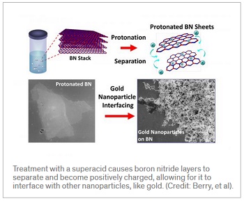
Researchers at the University of Illinois at Chicago have discovered a route to alter boron nitride, a layered 2D material, so that it can bind to other materials, like those found in electronics, biosensors and airplanes, for example. Being able to better-incorporate boron nitride into these components could help dramatically improve their performance.
The scientific community has long been interested in boron nitride because of its unique properties —it is strong, ultrathin, transparent, insulating, lightweight and thermally conductive — which, in theory, makes it a perfect material for use by engineers in a wide variety of applications. However, boron nitride’s natural resistance to chemicals and lack of surface-level molecular binding sites have made it difficult for the material to interface with other materials used in these applications.
UIC’s Vikas Berry and his colleagues are the first to report that treatment with a superacid causes boron nitride layers to separate into atomically thick sheets, while creating binding sites on the surface of these sheets that provide opportunities to interface with nanoparticles, molecules and other 2D nanomaterials, like graphene. This includes nanotechnologies that use boron nitride to insulate nano-circuits.
“Boron nitride is like a stack of highly sticky papers in a ream, and by treating this ream with chlorosulfonic acid, we introduced positive charges on the boron nitride layers that caused the sheets to repel each other and separate,” said Berry, associate professor and head of chemical engineering at the UIC College of Engineering and corresponding author on the paper.
“We showed that the positive charges on the surfaces of the separated boron nitride sheets make it more chemically active,” Berry said. “The protonation — the addition of positive charges to atoms — of internal and edge nitrogen atoms creates a scaffold to which other materials can bind.”
Berry said that the opportunities for boron nitride to improve composite materials in next-generation applications are vast.
“Boron and nitrogen are on the left and the right of carbon on the periodic table and therefore, boron-nitride is isostructural and isoelectronic to carbon-based graphene, which is considered a ‘wonder material,'” Berry said. This means these two materials are similar in their atomic crystal structure (isostructural) and their overall electron density (isoelectric), he said.
“We can potentially use this material in all kinds of electronics, like optoelectronic and piezoelectric devices, and in many other applications, from solar-cell passivation layers, which function as filters to absorb only certain types of light, to medical diagnostic devices,” Berry said.
Co-authors on the study are Sanjay Behura of UIC; Kabeer Jasuja of the Indian Institute of Technology; and Kayum Ayinde, Christina Wilson, Myles Ikenberry, Keith Hon and David Moore of Kansas State University.
Share on:


Testimonial
"We’re proud to call I-Connect007 a trusted partner. Their innovative approach and industry insight made our podcast collaboration a success by connecting us with the right audience and delivering real results."
Julia McCaffrey - NCAB GroupSuggested Items
Sealed for Survival: Potting Electronics for the Toughest Environments
10/29/2025 | Beth Massey, MacDermid Alpha Electronics SolutionsElectronics deployed in harsh conditions face relentless threats from vibration, impact, chemical contaminants, airborne pollutants, and moisture, conditions that can quickly lead to failure without robust protection. Potting, the process of encapsulating electronics in a protective polymer, is a widely used strategy to safeguard devices from both environmental and mechanical hazards.
Driving Innovation: Mechanical and Optical Processes During Rigid-flex Production
10/28/2025 | Kurt Palmer -- Column: Driving InnovationRigid-flex printed circuit boards are a highly effective solution for placing complex circuitry in tight, three-dimensional spaces. They are now indispensable across a range of industries, from medical devices and aerospace to advanced consumer electronics, helping designers make the most efficient use of available space. However, their unique construction—combining rigid and flexible materials—presents a fundamental challenge for PCB manufacturers.
SMTAI 2025 Review: Reflecting on a Pragmatic and Forward-looking Industry
10/27/2025 | Marcy LaRont, I-Connect007Leaving the show floor on the final afternoon of SMTA International last week in Rosemont, Illinois, it was clear that the show remains a grounded, technically driven event that delivers a solid program, good networking, and an easy space to commune with industry colleagues and meet with customers.
ITW EAE Despatch Ovens Now Support ASTM 5423 Testing
10/15/2025 | ITW EAEAs the demand for high-performance electrical insulation materials continues to grow—driven by the rapid expansion of electric vehicles (EVs) and energy storage systems—thermal processing has become a critical step in material development.
Beyond Thermal Conductivity: Exploring Polymer-based TIM Strategies for High-power-density Electronics
10/13/2025 | Padmanabha Shakthivelu and Nico Bruijnis, MacDermid Alpha Electronics SolutionsAs power density and thermal loads continue to increase, effective thermal management becomes increasingly important. Rapid and efficient heat transfer from power semiconductor chip packages is essential for achieving optimal performance and ensuring long-term reliability of temperature-sensitive components. This is particularly crucial in power systems that support advanced applications such as green energy generation, electric vehicles, aerospace, and defense, along with high-speed computing for data centers and artificial intelligence (AI).