


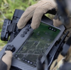


 American Made Advocacy: Smart Policies Can Ensure AI Data Centers Are Secure
 Beyond the Board: Early Engagement Means Faster Prototyping for Defense Programs
 Defense Speak Interpreted: The Autonomous Plane Battle—Skyborg Vs. Loyal Wingman


DARPA Announces Next Phase of Electronics Resurgence Initiative
November 5, 2018 | DARPAEstimated reading time: 3 minutes
First announced in June 2017, DARPA’s Electronics Resurgence Initiative (ERI) – a five-year, upwards of $1.5B investment in the future of domestic electronic systems – is rolling out the second phase of its research priorities. Comprised of several ongoing DARPA programs – including the six recently awarded ERI “Page 3” programs –ERI addresses long-foreseen obstacles to Moore’s Law and the challenges impeding 50 years of rapid progress in electronics advancement. The next phase of ERI will focus on further enmeshing the technology needs and capabilities of the defense enterprise with the commercial and manufacturing realities of the electronics industry.
ERI Phase II aims to address three key issues raised by the electronics community during a series of workshops that DARPA held during the San Francisco-based ERI Summit in July. These key issues are the need to support domestic manufacturing options and enable them to develop differentiated capabilities for diverse needs; a demand to invest in chip security; and a desire to create new connections between ERI programs as well as to demonstrate the resulting technologies in defense applications.
“Through ERI, DARPA is seeding the foundation of a more robust, secure, and heavily automated electronics industry to move us from an era of generalized hardware to specialized systems,” said Dr. Bill Chappell, director of DARPA’s Microsystems Technology Office (MTO). “The U.S. electronics industry has provided global leadership in the electronics arena since the invention of the transistor. The first phase of ERI was a major investment into the research and development required to stay competitive by exploring specialization with novel circuit materials, architectures, and designs. ERI Phase II seeks to build on that investment and push us toward a domestic semiconductor manufacturing sector that can implement specialized circuits; demonstrate that those circuits can be trusted through the supply chain and are built with security in mind; and are ultimately available to both DoD and commercial sector users.”
To create unique and differentiated domestic manufacturing capabilities, ERI Phase II will explore the addition of complementary and alternative vectors to traditional CMOS scaling. The first program in this space is Photonics in the Package for Extreme Scalability (PIPES), which will explore ways to bring the benefits of optical scaling directly to chips. PIPES will also work to establish a domestic ecosystem that facilitates long-term access to these new photonics capabilities for both commercial and DoD users. By significantly reducing the energy demands and challenges associated with moving data across digital microelectronics, the program could reduce the effort required to tie hundreds of GPUs together, and enable massive parallelism capable of supporting current and emerging data-intensive applications like machine learning, large-scale emulation, and advanced sensors.
Together with PIPES, other ERI Phase II investments are designed to ensure the development of novel manufacturing capabilities and support a strategy for the enduring availability of differentiated, high-performance electronics for the DoD and its commercial partners. This is important for the Department because its electronics manufacturing needs are numerous and diverse, and its systems have unique requirements and specific functionality. Although traditional CMOS scaling for digital processing is still an important area of investment, many critical DoD-relevant electronics will likely derive from alternative and complementary vectors. Potential areas of exploration under ERI Phase II include the integration of microelectromechanical systems (MEMS) and radiofrequency (RF) components directly into advanced circuits and semiconductor manufacturing processes. These efforts will build on the existing work in the ERI Materials & Integration research thrust, complementing current ERI programs like FRANC, 3DSoC, and CHIPS.
Throughout the remainder of 2018, DARPA plans to announce additional ERI Phase II investments relevant to issues highlighted at the ERI Summit. Potential areas of exploration include enabling the traceability of electronics components – from design to use – and the development of electronics that can enforce protections for security and privacy. Potential ERI Phase II programs will consider the need for assured electronics that incorporate protections from security risks. These efforts will build on ERI’s Design and Architectures research thrusts and leverage existing DARPA programs, such as SSITH that address hardware security and verification challenges.
ERI Phase II will also investigate ways to increase the connections between the various ERI efforts – from fundamental research programs to technology application programs – as well as emerging and future applications of ERI technologies developed across all sectors to defense-specific systems. These connections between programs and end users are key to ERI’s overall success, driving DARPA’s ability to deliver differentiated capabilities to the DoD and its partners. Programs under development should help ensure that the technological advances that derive from ERI will deliver significant impact for national security. Potential areas of exploration include ERI applications in large-scale physical emulation, cognitive RF systems, next-generation satellites, cybersecurity, and beyond.
To learn more about DARPA’s Electronics Resurgence Initiative, please click here.
Share on:


Testimonial
"The I-Connect007 team is outstanding—kind, responsive, and a true marketing partner. Their design team created fresh, eye-catching ads, and their editorial support polished our content to let our brand shine. Thank you all! "
Sweeney Ng - CEE PCBSuggested Items
SMT007 Magazine November 2025: Inside Mexico’s Rise as an Electronics Manufacturing Leader
11/03/2025 | I-Connect007 Editorial TeamMexico isn’t just part of the electronics manufacturing conversation—it’s leading it. From growing investments to cross-border collaborations, Mexico is fast becoming the center of electronics in North America. In this issue, we uncover why Mexico is earning global recognition. From top-ranked manufacturing capabilities to expanding partnerships that reach far beyond the U.S.
Henger Microelectronics Expands Global Footprint with Major Equipment Shipment to Southeast Asia
10/31/2025 |Henger Microelectronics has reached a major milestone in its global expansion strategy with the successful shipment of advanced plasma etching and cleaning systems, along with automation equipment, to multiple countries and regions across Southeast Asia. This achievement marks a significant step forward in the company’s international growth and reinforces its position as a leading force in the global plasma equipment industry.
TTCI Brings Hands-On Test Engineering and IPC Training Expertise to PCB Carolina 2025
10/31/2025 | The Test Connection Inc.The Test Connection Inc. (TTCI), a trusted provider of electronic test and manufacturing solutions, and The Training Connection LLC (TTC-LLC) will exhibit at PCB Carolina on Wednesday, November 12, 2025, at the McKimmon Center at NC State University in Raleigh, North Carolina. Attendees can visit Table 4 to say hello to Bert Horner and Bill Graver, and learn more about their test engineering services and technical training programs.
Cephia Secures $4M Seed Funding to Revolutionize Multimodal Sensing with Metasurface Technology
10/31/2025 | PRNewswireCephia, a startup building products using advanced AI computational imaging technologies and silicon sensors made from advanced metamaterials, formally launched with several pilot customers and $4 million in seed venture capital funding.
I-Connect007 Editor’s Choice: Five Must-Reads for the Week
10/31/2025 | Nolan Johnson, I-Connect007Last week, the IMPACT conference took place in Taipei, bringing together advanced packaging experts from around the globe to share their knowledge. We’ll be bringing you post-conference coverage over the next few weeks, so look for that in our newsletters, and in the Advanced Electronic Packaging Digest. Other news seemed to have the U.S. at the center of the global discussions. My picks start in Phoenix, where TSMC, NVIDIA, and Amkor are all scrambling to establish new capabilities. There’s nothing like a strong demand signal to cause build-out, and AI chips are doing exactly that.