


 American Made Advocacy: Rebuilding America’s Military Stockpiles Begins With Microelectronics
 The Right Approach: The End of an Era—DoD Proposes MIL-PRF-31032 Cancellation
 Defense Speak Interpreted: Hypersonics Report Back After Six Years of Silence


Physicists Design Next-Gen Antenna for Supersensitive Magnetic Field Detectors
November 6, 2018 | ITMO UniversityEstimated reading time: 2 minutes
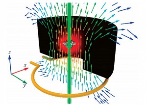
Scientists from ITMO University and the Lebedev Physical Institute of the Russian Academy of Sciences have proposed a new microwave antenna that creates a uniform magnetic field in large volume. It is capable of uniform and coherent addressing of the electronic spins of an ensemble of nanodiamond structure defects. This can be used to create super-sensitive magnetic field detectors of a new generation for magnetoencephalography in the study and diagnosis of epilepsy and other diseases. The results are published in JETP Letters.
Studying the characteristics of magnetic fields is necessary for many industries: from navigation to medicine. For example, magnetoencephalography can register magnetic fields that emerge as part of the brain’s function, as well as measure the activity of individual neurons. This method is used in the diagnosis of epilepsy and Alzheimer's disease, or in preparation for brain surgery. However, magnetoencephalography requires super-sensitive magnetometers: devices that record the properties of magnetic fields, even weak ones.
Therefore, scientists are constantly looking for new ways to create super-sensitive magnetometers of the new generation. Such devices should operate at room temperature and low input power. Moreover, they should be compact and relatively cheap. One of the promising options in this field is nanodiamonds with defects. Nanodiamonds are carbon nanostructures with a high refractive index and high thermal conductivity which almost do not interact with other substances. They may contain complex defects of the internal structure, such as Nitrogen-vacancy (NV) centers.
“Such defects may be created artificially: when a carbon atom is removed from the diamond's crystal lattice, the resulting vacancy is bonded to the implanted nitrogen atom. The structure of this defect is unique since the electronic spins of the individual center are manipulated by electromagnetic fields. Depending on the properties of the surrounding microwave magnetic field, the state of the electron spin of the NV-center is changing, and this can be recorded with optical methods,” explains Dmitry Zuev, researcher at the Faculty of Physics and Engineering at ITMO University.
However, as the response of a single NV-center is not strong enough, an ensemble of such defects is necessary in order to improve the sensitivity of sensors. This is where a problem arises, since the reaction of the electron spins of all the centers in the nanodiamond must be coherently addressed and manipulated. In other words, they must all be in a microwave magnetic field of the same intensity to ensure that their response is the same.
Scientists from ITMO University and Lebedev Physical Institute of the Russian Academy of Sciences suggested using a dielectric microwave antenna to coherently control the electron spins of NV-centers in the whole nanodiamond volume. The antenna is represented by a dielectric cylinder with an internal hole containing a nanodiamond with many NV-centers. This system is excited by an electric current. Once an input power of about 5 watts is applied, the dielectric cylinder creates a strong uniform magnetic field around the nanodiamond. As a result, the electron spins of all the NV-centers are synchronized in the same way and thus provide a high magnetometers sensitivity.
Measuring the Rabi frequency is the first step toward determining the sensitivity of the new magnetometer. Scientists plan to continue experiments and theoretical studies, searching for new antenna configurations that will provide even higher quality magnetometers.
Share on:


Testimonial
"In a year when every marketing dollar mattered, I chose to keep I-Connect007 in our 2025 plan. Their commitment to high-quality, insightful content aligns with Koh Young’s values and helps readers navigate a changing industry. "
Brent Fischthal - Koh YoungSuggested Items
Learning With Leo: What Is the Cost of Quality Brought About by Training?
12/03/2025 | Leo Lambert -- Column: Learning With LeoIn electronics manufacturing, conversations about training often revolve around one narrow question: What does it cost? Training requires time, materials, instructor fees, and occasionally travel. Under tight budget constraints, it is understandable that organizations scrutinize these expenses. However, this perspective misses a far more important and financially meaningful point: What is the cost of quality brought about by training? Framed differently: What does it cost when training does not occur?
Preventing Surface Prep Defects and Ensuring Reliability
06/10/2025 | Marcy LaRont, PCB007 MagazineIn printed circuit board (PCB) fabrication, surface preparation is a critical process that ensures strong adhesion, reliable plating, and long-term product performance. Without proper surface treatment, manufacturers may encounter defects such as delamination, poor solder mask adhesion, and plating failures. This article examines key surface preparation techniques, common defects resulting from improper processes, and real-world case studies that illustrate best practices.
I-Connect007 Editor’s Choice: Five Must-Reads for the Week
06/06/2025 | Nolan Johnson, I-Connect007Maybe you’ve noticed that I’ve been taking to social media lately to about my five must-reads of the week. It’s just another way we’re sharing our curated content with you. I pay special attention to what’s happening in our industry, and I can help you know what’s most important to read about each week. Follow me (and I-Connect007) on LinkedIn to see these and other updates.
The Chemical Connection: Reducing Defects in Circuit Board Production
06/04/2025 | Don Ball -- Column: The Chemical ConnectionWe all agree that in any manufacturing process, reducing defects in your product induced during manufacture (aka increasing yields) is a good thing. Doing so, however, can be a source of contention and frustration. I don’t pretend to be an expert in this field, because most of my work involves feasibility studies for new concepts or testing improvements made to existing equipment. High yields were usually not a factor; it’s simply about having enough data to prove or disprove a concept or seeing whether improvements to equipment design actually work. However, here are some observations I made visiting quality shops where high production at high yields was important.
Smart Automation: AI—Revolutionizing Inspection in Electronics Manufacturing
05/27/2025 | Josh Casper -- Column: Smart AutomationArtificial Intelligence (AI) is rapidly becoming a staple in our personal and professional lives. In electronics manufacturing, integrating AI to combat common inefficiencies and to contextualize data will open new doors into how we supplement our traditional processes. In some specific areas of the electronics manufacturing process, integration of AI on the factory floor is already having a tremendous effect. One such area is PCBA inspection, particularly 3D automated optical inspection (AOI) systems.