


 The Marketing Minute: If Your Marketing Budget Gets Cut in Half, Then What?
 Punching Out: How Are the Big Boys in Electronics Doing?
 It’s Only Common Sense: Complexity Is the Enemy of Profit


Atotech Experts to Present at SEMICON Europa and electronica 2018
November 9, 2018 | AtotechEstimated reading time: 2 minutes
Atotech Group will exhibit and present its latest products for power, automotive, and mobile semiconductor applications at this year’s SEMICON Europa. Atotech’s Semiconductor portfolio includes RDL and pillar plating solutions for next generation FOWLP and 5G applications as well as solutions for electroless pad metallization and double side plating for power semiconductors.
SEMICON Europa is the largest and most influential gathering for the semiconductor industry in Europe and attracts more thought leaders from overseas every year. This year the SEMICON show will be co-located with electronica, an equivalently important show for the printed circuit board and electronics assembly industry. Both events take place in Munich, Germany, from November 13 to 16, 2018. While hall A4 will be dedicated to SEMICON Europa, hall B5 will feature electronica.
Atotech’s product experts will be present at booth 569 in hall A4 to discuss latest technology, trends, and future requirements. This year’s product features include:
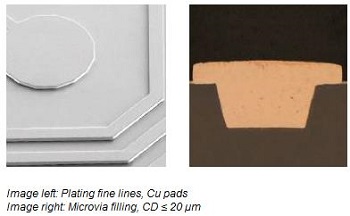
- Spherolyte Cu UF3 - High purity ECD copper process for fine line RDL plating and microvia filling capability
- Spherolyte Cu VR - Electrochemical copper process for fine line plating and simultaneous filling of various via dimensions
- Xenolyte Ni TR - A high-temperature resistant electroless nickel process for RDL and pad metallization
- Spherolyte Cu MD2 and MultiPlate - A new low stress ECD copper process for power semiconductors that is developed to run in Atotech's next generation semiconductor plating tool: MultiPlate
Atotech experts will also participate in the adjacent program with several presentations:
- On Tuesday, November 13, at 4:40 pm, Ulrich Memmert, Senior Scientist Material Sciences, will talk about “Mechanical properties of copper for advanced packaging” at the Strategic Materials Conference in Room 14a
- On Wednesday, November 14, at 12:55 p.m., Ralf Schmidt, R&D manager semiconductor, will introduce the audience to the “Enhanced mechanical properties of copper for Fan Out Wafer Level Packaging applications” at the Advanced Packaging Conference in Room 13b
- On Thursday, November 15, at 10:45 a.m., Markus Hoerburger, Global Product Manager Semiconductor & Functional Electronics Coatings, will talk about “Optimized Cu plating solution for next generation packaging" at the TechLounge on the Showfloor show floor in Hall A4
- Also on Thursday, November 15, at 4:35 p.m., Andreas Walter, Team Manager Semiconductor Electroless Processes, will discuss “Electroless ternary nickel alloys for under bump metallization (UBM) on power semiconductors for high temperature process conditions or applications” at the TechArena 2, hall A4
- As part of the adjacent electronica, Roger Massey, technical marketing manager, will present “Recent developments in advanced HDI PCBs” at the “PCB & Components marketplace” in Hall A1 on Friday, November 16, at 10:00 a.m..
Visitors to the show are invited to attend Atotech’s presentations and stop by at booth 569 in Hall A4 to discuss and elaborate on these and other topics and trends driving the industry.
About Atotech
Atotech is one of the world’s leading manufacturers of specialty chemicals and equipment for the printed circuit board, IC-substrate and semiconductor industries, as well as for the decorative and functional surface finishing industries. Atotech has annual sales of $1.2 billion (2017). The company is fully committed to sustainability – we develop technologies to minimize waste and to reduce environmental impact. Atotech has its headquarters in Berlin, Germany, and employs about 4,000 people in over 40 countries. For more information, click here.
Share on:


Testimonial
"Advertising in PCB007 Magazine has been a great way to showcase our bare board testers to the right audience. The I-Connect007 team makes the process smooth and professional. We’re proud to be featured in such a trusted publication."
Klaus Koziol - atgSuggested Items
I-Connect007 Releases The Printed Circuit Designer’s Guide to… Direct Metallization: A Guide to Complex PCB Fabrication
05/15/2026 | I-Connect007As PCB complexity continues to accelerate, fabricators and OEMs are reevaluating long-standing manufacturing processes to meet the demands of AI, HDI, advanced packaging, and next-generation electronics. To address these evolving challenges, I-Connect007 is proud to announce the release of The Printed Circuit Designer’s Guide to… Direct Metallization: A Guide to Complex PCB Fabrication, authored by MacDermid Alpha Solution’s Carmichael Gugliotti.
Driving Innovation: Selecting the Right Laser Source
04/28/2026 | Simon Khesin -- Column: Driving InnovationWhen I first joined Schmoll Maschinen, I brought experience from almost every PCB process, except for laser. As I immersed myself in laser processing, I realized why it can seem so daunting to a newcomer. The complexity arises from three intersecting factors: A vast variety of laser sources: CO2, UV-nano, green-pico, UV-pico, IR-pico, and others; a diverse range of applications: Drilling, cutting, ablation, and more; and an extensive list of materials: These have vastly different absorption rates. Choosing the right machine or laser source is rarely trivial. Even for experienced engineers, answering "Which source is best?" requires examining the business's specific goals.
Institute of Circuit Technology Spring Seminar 2026: A Bright Future in Europe
04/23/2026 | Pete Starkey, I-Connect007Through the leafy lanes and spring flowers of Warwickshire and back to Meridan, the traditional centre of England, and now officially part of the Metropolitan Borough of Solihull in the county of the West Midlands, I attended the Annual General Meeting and Spring Seminar of the Institute of Circuit Technology (ICT) on April 14. Out of the AGM came notable changes in leadership at the top of the Institute: the retirement of Mat Beadel as chair and Emma Hudson as technical director. Effective May 1, Steve Driver is the new chair, and Alun Morgan is the new technical director.
ACCM Unveils Negative and Near-zero CTE Materials for Large-Format AI Chips
04/21/2026 | Advanced Chip and Circuit MaterialsAdvanced Chip and Circuit Materials, Inc. (ACCM) has launched two new materials: Celeritas HM50, with a negative coefficient of thermal expansion (CTE) of -8 ppm/°C to offset the positive CTE and expansion of copper with temperature on circuit boards, and Celeritas HM001, with near-zero CTE and the low-loss performance needed for high-speed signal layers to 224 Gb/s and faster in artificial intelligence (AI) circuits.
Fresh PCB Concepts: Designing PCBs for Harsh Environments—Reliability Is Engineered Upstream
04/23/2026 | Team NCAB -- Column: Fresh PCB ConceptsWhen engineers hear the phrase “harsh environment,” they usually think of the extreme temperature swings, vibration and shock, pressure changes, or radiation in aerospace. However, aerospace is not the only harsh environment where electronic assemblies must survive. Automotive power electronics, downhole oil and gas tools, marine controls, rail systems, defense platforms, and industrial automation equipment all expose PCBs to environments that are equally unforgiving. The stress mechanisms may differ, but the physics does not.