


 The Marketing Minute: Marketing With Layers
 The Right Approach: Electro-Tek—A Williams Family Legacy, Part 1
 It’s Only Common Sense: If You’re Not Differentiated, You’re Dead


Crystallinity Reduces Resistance in All-Solid-State Batteries
November 27, 2018 | Tokyo Institute of TechnologyEstimated reading time: 2 minutes
Scientists at Tokyo Tech examined the mechanisms behind the resistance at the electrode-electrolyte interface of all-solid-state batteries. Their findings will aid in the development of much better Li-ion batteries with very fast charge/discharge rates.
Designing and improving lithium-ion (Li-ion) batteries is crucial for extending the limits of modern electronic devices and electric vehicles because Li-ion batteries are virtually ubiquitous. Scientists at Tokyo Tech, led by Prof. Taro Hitosugi, had previously reported a new type of all-solid-state battery, also based on lithium ions, which overcame one of the major problems of those batteries: high resistance at the interface between the electrodes and the electrolytes that limits fast charging/discharging.
Although the devices they produced were very promising and were much better than conventional Li-ion batteries in some regards, the mechanism behind the reduced interface resistance was unclear. It has been difficult to analyze the buried interfaces in all-solid-state batteries without damaging their layers. Therefore, Hitosugi and his team of researchers again investigated all-solid-state batteries to shed light on this topic. They suspected that crystallinity (which indicates how well-ordered and periodic a solid is) at the electrode-electrolyte interface played a key role in defining interface resistance.
To prove this, they fabricated two different all-solid-state batteries composed of electrode and electrolyte layers using a pulsed laser deposition technique (Fig. 1 and Fig. 2). One of these batteries had presumably high crystallinity at the electrode-electrolyte interface, whereas the other one did not. Confirming this was possible by using a novel technique called X-ray crystal truncation-rod scattering analysis. "X-rays can reach the buried interfaces without destroying the structures," explains Hitosugi.
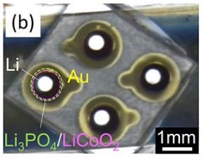
Figure 1. Structure of the thin-film all-solid-state batteries
The batteries were made by stacking thin films of Au (current collector), LiCoO2 (cathode), Li3PO4 (solid electrolyte), and Li (anode) on Al2O3 substrate. (a) Schematic cross-sectional view and (b) microscope photograph of the fabricated thin-film battery.
Figure 2. Conduction path of Li ions at the solid-electrolyte/electrode interface
(a) In the discharge process, Li ions migrate through the solid electrolyte to the interface. Since the LiCoO2 film is (0001)-oriented, the migration of Li ions into LiCoO2 is hindered by the CoO2 layers aligned parallel to the substrate surface. Therefore, Li ions migrate laterally on the surface of LiCoO2, and finally, diffuse into grain boundaries. (b) In the case of the disordered LiCoO2 surface, the diffusion of Li ions along the surface and into the grain boundary is restricted, resulting in a high interface resistance value.
Based on their results, the team concluded that a highly crystalline electrode-electrolyte interface resulted in low interface resistance, yielding a high-performance battery. By analyzing the microscopic structure of the interfaces of their batteries, they proposed a plausible explanation for the increased resistance of batteries with less crystalline interfaces. Lithium ions are stuck at the less crystalline interfaces, hindering ion conductivity. "Controlled fabrication of the electrolyte/electrode interface is crucial to obtain low interface resistance," explains Hitosugi. The development of theories and simulations to further understand the migration of Li ions will be crucial for finally achieving useful and improved batteries for all kinds of devices based on electrochemistry.
This work is carried out in collaboration with Prof. Susumu Shiraki at Nippon Institute of Technology and Senior Researcher Tetsuroh Shirasawa at the National Institute of Advanced Industrial Science and Technology.
Share on:


Testimonial
"Advertising in PCB007 Magazine has been a great way to showcase our bare board testers to the right audience. The I-Connect007 team makes the process smooth and professional. We’re proud to be featured in such a trusted publication."
Klaus Koziol - atgSuggested Items
Zuken Launches CR-8000 2025 with AI-Enhanced Support for High-Speed, High-Density PCB Design
05/21/2025 | ZukenZuken, a global leader in electronic design automation (EDA) solutions, has announced the release of the 2025 updates to its flagship PCB design applications, CR-8000 Design Gateway and Design Force.
RF PCB Design Tips and Tricks
05/08/2025 | Cherie Litson, EPTAC MIT CID/CID+There are many great books, videos, and information online about designing PCBs for RF circuits. A few of my favorite RF sources are Hans Rosenberg, Stephen Chavez, and Rick Hartley, but there are many more. These PCB design engineers have a very good perspective on what it takes to take an RF design from schematic concept to PCB layout.
IPC Announces New Training Course: PCB Design for Military & Aerospace Applications
12/23/2024 | IPCIPC announced the launch of a new training course: PCB Design for Military & Aerospace Applications.
eCADSTAR Sets New Standards for Compact PCB Design with Etched Inductor Parts
06/12/2024 | ZukenZuken announces the 2024 release of eCADSTAR, Zuken’s next-generation PCB design system for small and medium businesses. The new release includes a number of improvements ranging from enhanced design reuse, simplified revision tracking and more robust schematic design.
Elementary, Mr. Watson: Ensuring Design Integrity
03/28/2024 | John Watson -- Column: Elementary, Mr. WatsonBack in February, many of us watched the "Big Game." It reminded me of the saying, “It's not how you start that is important, but rather how you finish." It is perfectly okay when you are talking about sports, you get off to a bad first half and need to recover in the second half. However, when it comes to PCB design, this is not a good practice. If things start badly, they usually don't recover. They continue down that same path, costing more money and losing design time.