


 The Marketing Minute: Marketing With Layers
 The Right Approach: Electro-Tek—A Williams Family Legacy, Part 1
 It’s Only Common Sense: If You’re Not Differentiated, You’re Dead


Atomic Nitrogen Route to New 2D Semiconductors
December 3, 2018 | A*STAREstimated reading time: 2 minutes
A technique for making ultrathin, two-dimensional films of tungsten disulfide could underpin next-generation electronic and optoelectronic technologies.
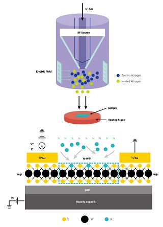
Image Caption: (Top) Schematic of the atomic nitrogen generation process with a RF plasma. (Bottom) Cross-sectional view of bottom-gated monolayer and few-layer WS2 FETs with Ti/Au contacts.
A simple and non-destructive fabrication technique could aid the manufacture of more energy efficient two-dimensional (2D) films needed to transform the electronics industry.
Atomically thin, 2D transition metal dichalcogenides (TMDCs) like tungsten disulfide (WS2) exhibit remarkable physical, electronic and optoelectronic properties, such as flexibility, transparency and semi-conducting characteristics.
Although there has been significant progress in fabricating 2D TMDCs, the ultrathin nature of such 2D semiconductors precludes the usage of techniques like ion implantation, with subsequent activation annealing, for introducing and retaining dopants within mono- or few-layer TMDCs.
Now, Dongzhi Chi and colleagues from the Institute of Materials Research and Engineering and the Institute of High Performance Computing at A*STAR, in collaboration with researchers from the National University of Singapore, have developed an innovative technique that uses highly reactive nitrogen (N) atoms for controlling dopants within films of WS2 at the atomic scale, and promises a reliable method for doping 2D TMDCs.
“[The current] inability to effectively dope 2D TMDCs hinders developing energy efficient devices like field-effect transistors using manufacturing technologies currently employed in the semiconductor industry,” says Chi.
TMDCs like WS2 are typically n-type semiconductors and there are currently no reliable methods for making atomically-thin TMDCs that are p-type. This is particularly vexing as it means that 2D TMDC devices, by necessity, are mostly based on n-type CMOS-FETs — field-effect transistors (FETs) fabricated using complementary metal-oxide-semiconductor (CMOS) technologies. The lack of an effective way to make p-type 2D TMDC-based CMOS-FETs limits the creation of next generation electronics, optoelectronic devices, and clean energy technologies.
So the researchers looked to atomic nitrogen as unlike current doping techniques, such as ion-implantation or plasma implantation, it can produce effective p-type doping in 2D TMDC-based CMOS-FETs without causing noticeable structural damage.
To produce atomic N, they used a plasma to generate ionized and atomic N in a ceramic cavity and applied an electrical field to retain the nitrogen ions, allowing the N atoms to react with a sample of WS2 heated to 300 degrees C.
The high chemical activity and low kinetic energy of the N introduced modifications to the structure at mono- or few-layer depth in the WS2 by replacing sulfur atoms and forming W-N chemical bonds. This proved to be ideal for controlling the dopants at the atomic scale.
“Unlike other doping methods for TMDCs —such as molecular chemisorption, physisorption and nitrogen plasma doping — our method introduces nitrogen into substitutional sites of sulfur by replacing the sulfur with nitrogen, without causing damage to the TMDC layers,” says Chi.
“Our work could help to accelerate the development of next generation electronics and optoelectronics technologies, such as ultralow power logic circuits and smart sensors, based on 2D semiconducting TMDCs,” says Chi.
Share on:


Testimonial
"In a year when every marketing dollar mattered, I chose to keep I-Connect007 in our 2025 plan. Their commitment to high-quality, insightful content aligns with Koh Young’s values and helps readers navigate a changing industry. "
Brent Fischthal - Koh YoungSuggested Items
Zuken Launches CR-8000 2025 with AI-Enhanced Support for High-Speed, High-Density PCB Design
05/21/2025 | ZukenZuken, a global leader in electronic design automation (EDA) solutions, has announced the release of the 2025 updates to its flagship PCB design applications, CR-8000 Design Gateway and Design Force.
RF PCB Design Tips and Tricks
05/08/2025 | Cherie Litson, EPTAC MIT CID/CID+There are many great books, videos, and information online about designing PCBs for RF circuits. A few of my favorite RF sources are Hans Rosenberg, Stephen Chavez, and Rick Hartley, but there are many more. These PCB design engineers have a very good perspective on what it takes to take an RF design from schematic concept to PCB layout.
IPC Announces New Training Course: PCB Design for Military & Aerospace Applications
12/23/2024 | IPCIPC announced the launch of a new training course: PCB Design for Military & Aerospace Applications.
eCADSTAR Sets New Standards for Compact PCB Design with Etched Inductor Parts
06/12/2024 | ZukenZuken announces the 2024 release of eCADSTAR, Zuken’s next-generation PCB design system for small and medium businesses. The new release includes a number of improvements ranging from enhanced design reuse, simplified revision tracking and more robust schematic design.
Elementary, Mr. Watson: Ensuring Design Integrity
03/28/2024 | John Watson -- Column: Elementary, Mr. WatsonBack in February, many of us watched the "Big Game." It reminded me of the saying, “It's not how you start that is important, but rather how you finish." It is perfectly okay when you are talking about sports, you get off to a bad first half and need to recover in the second half. However, when it comes to PCB design, this is not a good practice. If things start badly, they usually don't recover. They continue down that same path, costing more money and losing design time.