


 Trouble in Your Tank: Implementing Direct Metallization in Advanced Substrate Packaging
 It’s Only Common Sense: Storytelling That Sells—Stop Pitching, Start Painting Pictures
 The Right Approach: Get Ready for ISO 9001 Version 6


New Quantum Materials Could Take Computers Beyond the Semiconductor Era
December 4, 2018 | UC BerkeleyEstimated reading time: 5 minutes
Researchers from Intel Corp. and UC Berkeley are looking beyond current transistor technology and preparing the way for a new type of memory and logic circuit that could someday be in every computer on the planet.
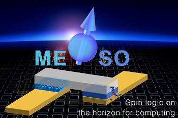
Image Caption: MESO devices, based on magnetoelectric and spin-orbit materials, could someday replace the ubiquitous semiconductor transistor, today represented by CMOS. MESO uses up-and-down magnetic spins in a multiferroic material to store binary information and conduct logic operations. (Intel graphic)
In a paper appearing online Dec. 3 in advance of publication in the journal Nature, the researchers propose a way to turn relatively new types of materials, multiferroics and topological materials, into logic and memory devices that will be 10 to 100 times more energy-efficient than foreseeable improvements to current microprocessors, which are based on CMOS (complementary metal–oxide–semiconductor).
The magneto-electric spin-orbit or MESO devices will also pack five times more logic operations into the same space than CMOS, continuing the trend toward more computations per unit area, a central tenet of Moore’s Law.
The new devices will boost technologies that require intense computing power with low energy use, specifically highly automated, self-driving cars and drones, both of which require ever increasing numbers of computer operations per second.
“As CMOS develops into its maturity, we will basically have very powerful technology options that see us through. In some ways, this could continue computing improvements for another whole generation of people,” said lead author Sasikanth Manipatruni, who leads hardware development for the MESO project at Intel’s Components Research group in Hillsboro, Oregon. MESO was invented by Intel scientists, and Manipatruni designed the first MESO device.
Transistor technology, invented 70 years ago, is used today in everything from cellphones and appliances to cars and supercomputers. Transistors shuffle electrons around inside a semiconductor and store them as binary bits 0 and 1.
Single crystals of the multiferroic material bismuth-iron-oxide. The bismuth atoms (blue) form a cubic lattice with oxygen atoms (yellow) at each face of the cube and an iron atom (gray) near the center. The somewhat off-center iron interacts with the oxygen to form an electric dipole (P), which is coupled to the magnetic spins of the atoms (M) so that flipping the dipole with an electric field (E) also flips the magnetic moment. The collective magnetic spins of the atoms in the material encode the binary bits 0 and 1, and allow for information storage and logic operations.
In the new MESO devices, the binary bits are the up-and-down magnetic spin states in a multiferroic, a material first created in 2001 by Ramamoorthy Ramesh, a UC Berkeley professor of materials science and engineering and of physics and a senior author of the paper.
“The discovery was that there are materials where you can apply a voltage and change the magnetic order of the multiferroic,” said Ramesh, who is also a faculty scientist at Lawrence Berkeley National Laboratory. “But to me, ‘What would we do with these multiferroics?’ was always a big question. MESO bridges that gap and provides one pathway for computing to evolve”.
In the Nature paper, the researchers report that they have reduced the voltage needed for multiferroic magneto-electric switching from 3 volts to 500 millivolts, and predict that it should be possible to reduce this to 100 millivolts: one-fifth to one-tenth that required by CMOS transistors in use today. Lower voltage means lower energy use: the total energy to switch a bit from 1 to 0 would be one-tenth to one-thirtieth of the energy required by CMOS.
“A number of critical techniques need to be developed to allow these new types of computing devices and architectures,” said Manipatruni, who combined the functions of magneto-electrics and spin-orbit materials to propose MESO. “We are trying to trigger a wave of innovation in industry and academia on what the next transistor-like option should look like.”
Page 1 of 2
Share on:


Testimonial
"The I-Connect007 team is outstanding—kind, responsive, and a true marketing partner. Their design team created fresh, eye-catching ads, and their editorial support polished our content to let our brand shine. Thank you all! "
Sweeney Ng - CEE PCBSuggested Items
Panasonic Industry will Double the Production Capacity of MEGTRON Multi-layer Circuit Board Materials Over the Next Five Years
09/15/2025 | Panasonic Industry Co., Ltd.Panasonic Industry Co., Ltd., a Panasonic Group company, announced plans for a major expansion of its global production capacity for MEGTRON multi-layer circuit board materials today. The company plans to double its production over the next five years to meet growing demand in the AI server and ICT infrastructure markets.
Trouble in Your Tank: Implementing Direct Metallization in Advanced Substrate Packaging
09/15/2025 | Michael Carano -- Column: Trouble in Your TankDirect metallization systems based on conductive graphite are gaining popularity throughout the world. The environmental and productivity gains achievable with this process are outstanding. Direct metallization reduces the costs of compliance, waste treatment, and legal issues related to chemical exposure. A graphite-based direct plate system has been devised to address these needs.
Fresh PCB Concepts: Designing for Success at the Rigid-flex Transition Area
08/28/2025 | Team NCAB -- Column: Fresh PCB ConceptsRigid-flex PCBs come in all shapes and sizes. Manufacturers typically use fire-retardant, grade 4 (FR-4) materials in the rigid section and flexible polyimide materials in the flex region. Because of the small size, some rigid-flex PCBs, like those for hearing aid devices, are among the most challenging to manufacture. However, regardless of its size, we should not neglect the transition area between the rigid and flexible material.
Global Sourcing Spotlight: How to Evaluate Supplier Capabilities Worldwide
08/20/2025 | Bob Duke -- Column: Global Sourcing SpotlightIn global sourcing, the difference between a competitive edge and a catastrophic disruption often comes down to how well you vet your suppliers. Sourcing advanced PCBs, precision components, or materials for complex assemblies demands diligence, skepticism, and more than a little time on airplanes. Here’s how to do your due diligence when evaluating international suppliers and why cutting corners can cost you more than money.
Insulectro and Electroninks Sign North American Distribution Agreement
08/12/2025 | InsulectroElectroninks, a leader in metal organic decomposition (MOD) inks for additive manufacturing and advanced semiconductor packaging, today announced a strategic collaboration and distribution partnership with Insulectro, a premier distributor of materials used in printed electronics and advanced interconnect manufacturing.