


 The Marketing Minute: Marketing With Layers
 The Right Approach: Electro-Tek—A Williams Family Legacy, Part 1
 It’s Only Common Sense: If You’re Not Differentiated, You’re Dead


Form-Fitting, Nanoscale Sensors Now Make Sense
December 6, 2018 | Rice UniversityEstimated reading time: 3 minutes
What if a sensor sensing a thing could be part of the thing itself? Rice University engineers believe they have a two-dimensional solution to do just that.
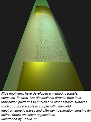
Rice engineers led by materials scientists Pulickel Ajayan and Jun Lou have developed a method to make atom-flat sensors that seamlessly integrate with devices to report on what they perceive.
Electronically active 2D materials have been the subject of much research since the introduction of graphene in 2004. Even though they are often touted for their strength, they’re difficult to move to where they’re needed without destroying them.
The Ajayan and Lou groups, along with the lab of Rice engineer Jacob Robinson, have a new way to keep the materials and their associated circuitry, including electrodes, intact as they’re moved to curved or other smooth surfaces.
The Rice team tested the concept by making a 10-nanometer-thick indium selenide photodetector with gold electrodes and placing it onto an optical fiber. Because it was so close, the near-field sensor effectively coupled with an evanescent field – the oscillating electromagnetic wave that rides the surface of the fiber—and accurately detected the flow of information inside.
The benefit is that these sensors can now be imbedded into such fibers where they can monitor performance without adding weight or hindering the signal flow.
“This paper proposes several interesting possibilities for applying 2D devices in real applications,” Lou said. “For example, optical fibers at the bottom of the ocean are thousands of miles long, and if there’s a problem, it’s hard to know where it occurred. If you have these sensors at different locations, you can sense the damage to the fiber.”
Lou said labs have gotten good at transferring the growing roster of 2D materials from one surface to another, but the addition of electrodes and other components complicates the process. “Think about a transistor,” he said. “It has source, drain and gate electrodes and a dielectric (insulator) on top, and all of these have to be transferred intact. That’s a very big challenge, because all of those materials are different.”
Raw 2D materials are often moved with a layer of polymethyl methacrylate (PMMA), more commonly known as Plexiglas, on top, and the Rice researchers make use of that technique. But they needed a robust bottom layer that would not only keep the circuit intact during the move but could also be removed before attaching the device to its target. (The PMMA is also removed when the circuit reaches its destination.)
The ideal solution was polydimethylglutarimide (PMGI), which can be used as a device fabrication platform and easily etched away before transfer to the target. “We’ve spent quite some time to develop this sacrificial layer,” Lou said. PMGI appears to work for any 2D material, as the researchers experimented successfully with molybdenum diselenide and other materials as well.
The Rice labs have only developed passive sensors so far, but the researchers believe their technique will make active sensors or devices possible for telecommunication, biosensing, plasmonics and other applications.
Rice graduate student Zehua Jin is lead author of the paper. Co-authors are Rice graduate students Fan Ye, Shuai Jia and Liangliang Dong and postdoctoral researcher Xiang Zhang; Rice alumnus Sidong Lei, now an assistant professor at Georgia State University, and Robert Vajtai, a research professor in materials science and nanoengineering at Rice. Ajayan is chair of Rice’s Department of Materials Science and NanoEngineering, the Benjamin M. and Mary Greenwood Anderson Professor in Engineering and a professor of chemistry. Lou is a professor of materials science and nanoengineering. Robinson is an assistant professor of electrical and computer engineering.
The research was supported by the Air Force Office of Scientific Research, the Welch Foundation, Rice IDEA and Function Accelerate nanoMaterial Engineering (FAME), one of six centers of the Semiconductor Technology Advanced Research Network sponsored by the Microelectronics Advanced Research Corporation and the Defense Advanced Research Projects Agency.
Share on:


Testimonial
"The I-Connect007 team is outstanding—kind, responsive, and a true marketing partner. Their design team created fresh, eye-catching ads, and their editorial support polished our content to let our brand shine. Thank you all! "
Sweeney Ng - CEE PCBSuggested Items
ITW EAE Despatch Ovens Now Support ASTM 5423 Testing
10/15/2025 | ITW EAEAs the demand for high-performance electrical insulation materials continues to grow—driven by the rapid expansion of electric vehicles (EVs) and energy storage systems—thermal processing has become a critical step in material development.
Beyond Thermal Conductivity: Exploring Polymer-based TIM Strategies for High-power-density Electronics
10/13/2025 | Padmanabha Shakthivelu and Nico Bruijnis, MacDermid Alpha Electronics SolutionsAs power density and thermal loads continue to increase, effective thermal management becomes increasingly important. Rapid and efficient heat transfer from power semiconductor chip packages is essential for achieving optimal performance and ensuring long-term reliability of temperature-sensitive components. This is particularly crucial in power systems that support advanced applications such as green energy generation, electric vehicles, aerospace, and defense, along with high-speed computing for data centers and artificial intelligence (AI).
Is Glass Finally Coming of Age?
10/13/2025 | Nolan Johnson, I-Connect007Substrates, by definition, form the base of all electronic devices. Whether discussing silicon wafers for semiconductors, glass-and-epoxy materials in printed circuits, or the base of choice for interposers, all these materials function as substrates. While other substrates have come and gone, silicon and FR-4 have remained the de facto standards for the industry.
Creative Materials to Showcase Innovative Functional Inks for Medical Devices at COMPAMED 2025
10/09/2025 | Creative Materials, Inc.Creative Materials, a leading manufacturer of high-performance functional inks and coatings, is pleased to announce its participation in COMPAMED 2025, taking place November 17–20 in Düsseldorf, Germany.
Jiva Leading the Charge Toward Sustainable Innovation
09/30/2025 | Marcy LaRont, PCB007 MagazineEnvironmental sustainability in business—product circularity—is a high priority these days. “Circularity,” the term meant to replace “recycling,” in its simplest definition, describes a full circle life for electronic products and all their elements. The result is re-use or a near-complete reintroduction of the base materials back into the supply chain, leaving very little left for waste. For what cannot be reused productively, the ultimate hope is to have better, less harmful means of disposal and/or materials that can seamlessly and harmlessly decompose and integrate back into the natural environment. That is where Jiva and Soluboard come in.