


 The Marketing Minute: Marketing With Layers
 The Right Approach: Electro-Tek—A Williams Family Legacy, Part 1
 It’s Only Common Sense: If You’re Not Differentiated, You’re Dead


NIST’s Antenna Evaluation Method Could Help Boost 5G Network Capacity and Cut Costs
December 11, 2018 | NISTEstimated reading time: 2 minutes
Researchers at the National Institute of Standards and Technology (NIST) have developed a method for evaluating and selecting optimal antenna designs for future fifth-generation (5G) cellphones, other wireless devices and base stations.
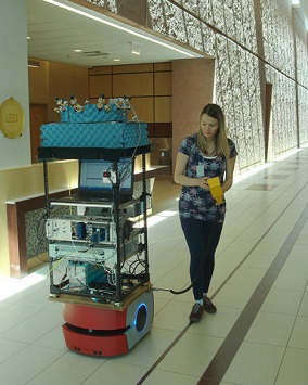
Image Caption: NIST researcher Jelena Senic drives a robot used to measure the performance of different antenna beam patterns. The mobile platform enables researchers to position a wireless channel sounder that includes (top to bottom) an array of 16 receive antennas, the receiver, timing circuitry, a signal digitizer and a battery for untethered field operations.
The new NIST method could boost 5G wireless network capacity and reduce costs.
5G systems will avoid crowded conventional wireless channels by using higher, millimeter-wave frequency bands. Transmissions at these frequencies lose a lot of energy along the way, which weakens received signal strength. One solution is “smart” antennas that can form unusually narrow beams—the area in space where signals are transmitted or received—and rapidly steer them in different directions.
Antenna beamwidth affects wireless system design and performance. NIST’s new measurement-based method allows system designers and engineers to evaluate the most appropriate antenna beamwidths for real environments.
“Our new method could reduce costs by enabling greater success with initial network design, eliminating much of the trial and error that is now required,” NIST engineer Kate Remley said. “The method also would foster the use of new base stations that transmit to several users either simultaneously or in rapid succession without one antenna beam interfering with another. This, in turn, would increase network capacity and reduce costs with higher reliability.”
This is the first detailed measurement-based study of how antenna beamwidth and orientation interact with the environment to affect millimeter-wave signal transmission. In the technique, NIST measurements covering a broad range of antenna beam angles are converted into an omnidirectional antenna pattern covering all angles equally. The omnidirectional pattern can then be segmented into narrower and narrower beamwidths. Users can evaluate and model how antenna beam characteristics are expected to perform in specific types of wireless channels.
An engineer could use the method to select an antenna that best suits a specific application. For example, the engineer may choose a beamwidth that is narrow enough to avoid reflections off certain surfaces or that allows multiple antennas to coexist in a given environment without interference.
To develop the new method, the NIST team collected experimental data in a hallway and lobby of a NIST research building, using a special robot loaded with a customized channel sounder and other equipment. A channel sounder collects data that capture the signal reflections, diffractions and scattering that occur between a transmitter and receiver. Many such measurements can be used to create a statistical representation of the radio channel, to support reliable system design and standardization.
NIST study results confirm that narrow beams can significantly reduce signal interference and delays, and that an optimized beam orientation reduces energy loss during transmissions. For example, the time interval during which signal reflections arrive (a metric called RMS delay spread) dropped dramatically from 15 nanoseconds (ns) to about 1.4 ns as antenna beamwidth was reduced from omnidirectional (360 degrees) to a narrow 3 degrees or so-called pencil beam.
Future research will include extending the method to different environments and analysis of other wireless channel characteristics.
Share on:


Testimonial
"We’re proud to call I-Connect007 a trusted partner. Their innovative approach and industry insight made our podcast collaboration a success by connecting us with the right audience and delivering real results."
Julia McCaffrey - NCAB GroupSuggested Items
Elementary Mr. Watson: Chasing Checkmarks, Not Signal Integrity
10/01/2025 | John Watson -- Column: Elementary, Mr. WatsonFor the September 2025 issue of Design007 Magazine on signal integrity, I explored how the PCB is similar to a military obstacle course: walls that sap energy like impedance mismatches, barbed wire that cuts like crosstalk, and mud pits that drag a signal down like attenuation. The takeaway was clear that a PCB is not a flat drawing; it's an electromagnetic ecosystem filled with hazards that test every signal that dares to cross it. The real danger lies not in the obstacles themselves, but in the fact that many designers never see them.
Signal Integrity: A Game of Margins
09/25/2025 | Andy Shaughnessy, Design007 MagazineAs the founder of Wild River Technology, Al Neves deals with some of the most challenging aspects of signal integrity. Wild River’s engineers consult with high-tech companies that work at very high speeds and frequencies, often above 100G. Al is always a fun interview, so we asked him to share his thoughts on the current state of signal integrity engineering.
Understanding Signal Integrity, the Foundation of High-Speed Digital Design
09/25/2025 | Stephen V. Chavez, Siemens EDASignal integrity has become a critical factor in ensuring reliable performance in high-speed digital systems. As data rates continue to increase, engineers must understand the fundamental principles that govern how signals propagate through transmission lines and how to mitigate common issues that can degrade signal quality.
Beyond Design: Slaying Signal Integrity Villains
09/17/2025 | Barry Olney -- Column: Beyond DesignHigh-speed PCB design is a balancing act, where subtle oversights can develop into major signal integrity nightmares. Some culprits lie dormant during early validation, only to reveal themselves later through workflow disruptions and elusive performance bottlenecks. Take crosstalk, for example. What begins as a stray signal coupling between traces can ripple through the design, ultimately destabilizing the power distribution network. Each of these troublemakers operates with signature tactics, but they also have well-known vulnerabilities.
Staying on Top of Signal Integrity Challenges
09/16/2025 | Andy Shaughnessy, Design007 MagazineOver the years, Kris Moyer has taught a variety of advanced PCB design classes, both online IPC courses and in-person classes at California State University-Sacramento, where he earned his degrees in electrical engineering. Much of his advanced curriculum focuses on signal integrity, so we asked Kris to discuss the trends he’s seeing in signal integrity today, the SI challenges facing PCB designers, and his go-to techniques for controlling or completely eliminating SI problems.